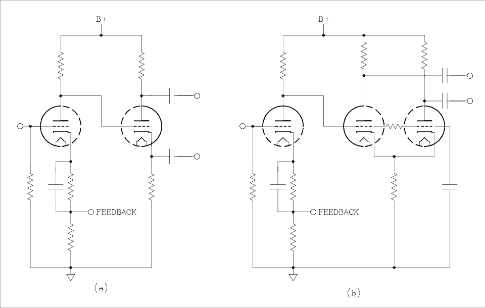
Figure 1 Two Typical Phase Inverters.
For a verbal description click here.
Learning LT Spice.
After putting it off for literally years I am finally making a determined effort to learn spice. Specifically, LT Spice because it is still free. It may well be the most complex, most difficult to learn, and most powerful circuit simulator around. As such it should be fairly accurate. Well, I am told that it depends on the models. Since we are having fun with tubes we need tube models for spice. I have been provided with a set of models that I am told are very good. Well why don't we see about that. I have spent hundreds of hours taking data on real circuits and posting that data on this website. Now I'm going to simulate these circuits to see how well the spice simulations match the real world data. At this writing I haven't done any simulations so I don't know how things will come out. But good, bad, or ugly, I will post them as they are without any fudging or excuses. Like this paragraph the new data will be in red.The tube models mentioned in the paragraph above did not include the 6DJ8 or 12AV7 both of which are used prominently in this article. I was given models for these tubes with the caveat "use at your own risk". With that in mind, onward we sail.
Improving the Phase Inverter.
If I were to collect all the writing I have done on phase inverters I could probably turn it into a book. And this is it.Much has been written by others and myself on the subject of phase inverters. At the moment John Wise, Tim E. Smith (don't call him Timmy) , and I are working more or less independently on improving the part of the amplifier that comes before the power tubes. In its simplest form it consists of an amplifier stage and a phase inverter. It can get very complicated but is the complication worth the effort? In this article I will attempt to answer that question and a few others.
Purpose.
The purpose of this research project is to examine two often used phase inverter circuits and investigate means of reducing distortion while producing a sufficient output voltage to drive most types of power tubes to full output. The two circuits to be investigated are the split load phase inverter (SLPI) and the long tail pair (LTP).The Split Load Phase Inverter (SLPI).
First the SLPI alone will be evaluated using several tube types to determine its distortion characteristics. The tests will be made at 4 different voltage output levels which have been deemed to be typical of real amplifier service.Next an amplifier stage will be added before the SLPI and the resulting circuit tested as a whole. Distortion reducing measures will be added to the preinverter amplifier such as local negative feedback and bootstrapping the plate load resistor. Both triodes and pentodes will be tested.
The amount of gain the inverter/driver* is required to supply depends on how much global negative feedback (GNFB) is applied to the amplifier. Specifically, 20 dB, 10 dB, or 0 dB. The inverter/driver will be evaluated at gain values that are suitable for combinations of the amount of GNFB and drive requirements of the power tubes.
* The term "inverter/driver" is used to refer to the combination of the phase inverter and all amplifier stages, except voltage amplifiers that are outside the global feedback loop and power amplifier tubes. In general the inverter/driver" is found between the point where GNFB is injected, and the grids of the output tubes.Next a postinverter amplifier, ala the Williamson circuit, will be added. This amplifier will be modified in ways intended to reduce its distortion.
Finally a heavily bootstrapped Williamson circuit submitted by John Wise will be Breadboarded and tested for distortion and bandwidth.
The Long Tail Pair. (LTP)
First the long tail pair (LTP) will be evaluated by itself. Unlike the SLPI the LTP has gain greater than unity and this will be evaluated for use in a practical amplifier. Modifications suggested by Tim E. Smith will be applied to reduce distortion.Then the preinverter amplifier will be added and the circuit tested as a whole. Again Smith modifications will be performed on the amplifier stage to reduce distortion.
Goals.
- To build an "inverter/driver" with total harmonic distortion less than 0.15%.
- To build an "inverter/driver" with amplifier gain that can be adjusted for the proper value by altering a resistor value or adjusting a potentiometer without altering the operating point of any of the tubes.
- To build an "inverter/driver" that contains a minimum of low frequency RC roll offs. One would be ideal but appears unobtainable. Two is the goal but that too may be difficult to achieve.
- To build an "inverter/driver" with vacuum tube technology where possible but not be afraid to use such items as MOSFETs and zener diodes especially where they can keep the tube count from getting out of hand.
Time Line.
The text, tables, and schematic diagrams have been arranged so the article flows smoothly and logically. The experimental work was not so logically organized. The initial order was as follows.
1. The long tail pair.
2. The split load phase inverter.
3. The Williamson circuit.
4. The Wise - Williamson circuit.
But while optimizing the Wise - Williamson circuit I learned something which I thought could improve both the split load phase inverter and the Williamson circuit. So I went back and tried to rework some of those circuits. I found that I could not improve on the performance of the circuits so I decided to let well enough alone.What is a phase inverter?
There are phase inverters and phase splitters and on other pages in this site I have endeavored to be consistent. Strictly speaking a phase inverter is any circuit that produces two signals of equal amplitude and opposite phase.A phase splitter is shorthand for a "split load phase inverter" (SLPI). In modern times this circuit seems to have acquired other names which are not descriptive of the function. In my universe the forgoing is its name. Note that the full name includes the words "phase inverter". All phase splitters are phase inverters but all phase inverters are not phase splitters.
Note: I always prefer a name which, if possible, is in some way descriptive of the function.For a quick review here are the two basic circuits we will be considering.
Figure 1 Two Typical Phase Inverters.
For a verbal description click here.
These are not meant to cover all possible phase inverter circuits. The two circuits are representative of the two most used circuits, the SLPI (split load phase inverter) a, and the (LTP) long tail pair b.
Figure 1a is often found with a coupling capacitor between the plate of the first tube and the grid of the second. In this case other means are provided for biasing the second tube. Also the first tube may be a pentode instead of a triode. This gives increased gain at the cost of increased complication and distortion. Also the plate load of the first tube may be some kind of constant current source or bootstrapped resistor. It is assumed that this improves linearity and therefor decreases distortion. It also increases gain but it also increases complexity. Because the gain of the SLPI is slightly less than unity all of the gain in the circuit has to come from the first tube. If this amplifier stage can't be coaxed into producing enough gain, another gain stage is added after the SLPI as in the Williamson circuit.
Figure 1b is usually seen as drawn. When a resistor is used in the cathode unequal load resistors are required for the two triodes to provide equal signal voltages. A current sink may be used in the cathode circuit in which case the plate loads are equal. This circuit has an advantage in that both stages contribute gain greater than unity. The first triode is one stage and the other two triodes taken together form the second stage. Because gains multiply it isn't hard to get enough gain for a 20 dB feedback loop.
Requirements for a Phase inverter.
As you will learn in paragraphs below the reputation of the 6DJ8 is well deserved. I must admit that I used to think that all the hullabaloo surrounding this tube was just so much hype. It is clear from data collected that the tube is for real. Its high price is a result of basic economics, high demand and short supply. Anyone who wants one must pay the price or go without.I can now realistically think about an amplifier with no global negative feedback (GNFB). Or if zero GNFB can't reach the goal maybe one with only 10 dB of GNFB. Let's take a look at Table 1 and see how much inverter/driver gain we need for 20 dB, 10 dB, and 0 dB of GNFB.
Table 1
Required Gain and Output From inverter/driver for a Few Common Power Tubes.Tube Type Power
Output (W)Drive, Each
Power Tube.
(RMS Volts)Inverter/Driver
Gain For
20 dB GNFBInverter/Driver
Gain For
10 dB GNFBInverter/Driver
Gain For
0 dB GNFB6V6GT 14 10.6 106 33.5 10.6 6L6/G/GT 26.5 15.9 159 50.3 15.9 6L6GC 55 24.7 247 78.1 24.7 EL34 54 25 250 79 25 EL34 UL 34 25 250 79 25 6550 EBB=400V 55 17 170 53.8 17 6550 EBB=600V 100 23 230 72.7 23 This opens up a Pandora's box of circuits and tube types. So many in fact that I couldn't possibly examine every one. I do want to finish this article before they have my funeral.
Practical Limitations on SLPI Output.
So let's go with the gold and use a 6DJ8 for the SLPI. After all we only need one for a stereo amplifier. That means we will assume a gain of 0.93 for the SLPI. If we use a bootstrapped 12AX7 as the preinverter stage we can get an overall gain of 93. If we use this combination with the 6V6 class of tubes and approximate the drive voltage as 10 the input for full power will be 10*10/93 which is approximately 1.08 volts for full power.If we try to do this with the 6L6GC - 6550 class of output voltage we will find the input voltage for full power greatly exceeds 1 volt. If we were going to always use 20 dB of GNFB the above decision would eliminate the need to take data for the 17 and 25 volt output level. In order to keep the possibility of 10 dB or even no GNFB open I am going to take data for all 4 output voltages. In some preliminary testing it was found that the distortion using 68 k ohm resistors was quite high so data will not be tabulated for this resistance value.
In addition 4 individuals of each tube type will be tested. This may remove the possibility of lucking into an extremely good tube.
Evaluating the Split Load Phase Inverter in Isolation.
Now that we know how much output we need from the SLPI we can test the circuit with various tubes to see how they behave. As stated above I have selected four key voltages for the test, 1.5, 10, 17 and 25 volts RMS per output. 1.5 volts approximates the operating level of the SLPI which is in the middle of a Williamson inverter/driver circuit. 10 volts approximates the drive for a pair of 6V6GTs. 17 volts is exactly the value needed to drive a pair of 6550s to 55 watts and approximates the drive for a pair of 6L6/G/GTs. 25 volts takes care of the rest of the tubes listed in table 1 either approximately or exactly.
Figure 2 Split Load Phase Inverter Test Circuit.
For a verbal description click here.
To evaluate the SLPI operating all by itself I need an audio generator that will deliver a maximum of 25 volts. (Note: I actually need more than that because for the worst case I need to make measurements at 25 volts output. Because the SLPI has a gain of less than unity I need more than that.) Fortunately I have an HP 200CD, I got from J. Ed. It used to belong to the Fender company. As it arrived in my shop its maximum output was set to 19 volts. It's distortion measured at 0.04%.I think Ed adjusted it to that value for minimum distortion or possibly as a reasonable compromise between output and distortion. A note on the schematic says to adjust the amplitude pot for 24 volts output. I have chosen to interpret the setting as optional. I trimmed up the maximum output adjustment for an output of 20 volts. The distortion remained at 0.04% and a couple of weeks later it still gave the same reading. After about 45 minutes of warmup the distortion settled at 0.048%. After about an hour the reading of distortion, with the oscillator connected directly to the analyzer, started jumping erratically. This was a condition I couldn't live with so there was nothing for it but to put the HP oscillator on the bench for service.
I changed all the tubes, yes I have spares on hand, applied contact cleaner to the rotor grounds on the variable capacitor, Cleaned the bases of the stabilizing lamps and made sure they were tight in their sockets. To my shock the distortion was up to 0.12%. Low distortion must depend on matched tubes. So I started swapping tubes. Long story a little shorter I achieved 0.045 which rose to 0.048 after about 2 hours of warmup. There was no jumping. I'll never know which of the three things I did cured it but I didn't want to take the time to change one thing at a time followed by a 2 hour bench test for each one. After a cooldown and 2 hour warmup the distortion settled at 0.052%. I can live with that.
Then I started taking data. The HP 200 was used for the 10, 17, and 25 volt tests. The Siglent SDG810 was used for the 1.5 volt tests. When the 810 was connected directly to the distortion analyzer the reading was 0.03%. But as I ran through the tests on the circuit some of the readings were 0.028 or 0.026. "That's impossible'" I told myself. I also told the analyzer but it persisted in giving me the same readings. Then I thought of it. The generator must have been putting out spurious signals and/or digital noise that were in the frequency band of the analyzer but above the upper limit of the amplifier. I realized that I needed to filter out everything above the test frequency. So I built a passive network in a little box that terminates the generator and attenuates frequencies above 1000 Hz. With the generator connected directly to the analyzer it now reads 0.022%. That's 73.2 dB down from 100%. The noise floor of the analyzer is at 0.006%. That's 84.4 dB down from 100%.
About the Tubes.
All of the 6DJ8s I have, came in boxes that did not have the tube number printed or written on the outside. The number is in my hand printing. Looking at the tubes, tube 1 is a Tung Sol. Tubes 2, 3, and 4 are labeled as shown in the picture. If you can figure it out pleas share the knowledge with me and I will add it to this page.J. E. Knox was first to interpret the sloppy printing for me. It reads, "ECC88/6DJ8 MADE IN W.GERMANY". Technically speaking it was made in a country that doesn't exist anymore.
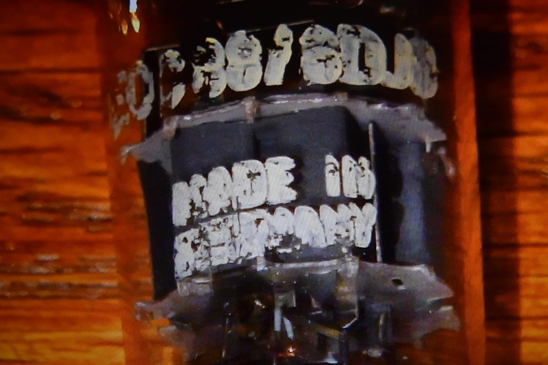
Photo showing tube with sloppily painted characters.
I selected these two tubes for tabulation because in preliminary tests these two were the best out of several twin triodes evaluated.
There are two lots of the 12AV7. Tubes 1 and 4 are Raytheon and the condition of their boxes indicates they were manufactured recently, as tubes go. Tube 2 is a Tung Sol and 3 is an RCA. They both came with me from Florida in 1968 and their boxes are falling apart.
Table 2
Split Load Phase Inverter, Ebb = 400 volts.Tube Rk & Rb # Vk for Min %D @Vo
1.5V/10V/17V/25VGain %D @ Vo = 1.5 V
Plate/Cathode%D @ Vo = 10 V
Plate/Cathode%D @ Vo = 17 V
Plate/Cathode%D @ Vo = 25 V
Plate 1/Plate 26DJ8 15 kΩ 1 100/100/100/122 0.942 ~0.045/TSM ~0.067/0.063 ~0.074/0.061 ~0.086/0.086 2 90/100/100/115 0.923 TSM/TSM ~0.062/0.054 ~0.076/0.060 ~0.108/0.092 3 90/100/100/100 0.929 TSM/TSM ~0.066/0.058 ~0.076/0.066 ~0.096/0.086 4 90/100/122/*122 0.960 TSM/TSM ~0.066/0.059 ~0.099/0.078 ~*0.116/0.111 22 kΩ 1 100/100/106/100 0.968 TSM/TSM ~0.057/0.057 ~0.058/0.050 ~0.113/0.156 2 100/100/110/108 0.943 TSM/TSM ~0.058/0.057 ~0.055/0.046 ~0.112/0.117 3 100/100/115/118 0.932 TSM/TSM ~0.039/0.039 ~0.050/0.042 ~0.111/0.117 4 100/100/120/120 0.949 TSM/TSM ~0.45/0.41 ~0.077/0.066 ~0.134/0.136 33 kΩ 1 100/100/113/117 0.938 TSM/TSM ~TSM/0.025 ~0.044/0.044 ~0.115/0.126 2 100/100/120/115 0.909 TSM/TSM ~TSM/0.029 ~0.045/0.044 ~0.126/0.132 3 100/100/122/121 0.915 TSM/TSM ~TSM/0.025 ~0.039/0.039 ~0.115/0.126 4 100/100/123/122 0.932 TSM/TSM ~0.038/0.040 ~0.070/0.064 ~0.135/0.147 47 kΩ 1 100/122/125/121 0.920 TSM/TSM ~TSM/0.027 ~028/0.037 ~0.043/0.070 2 100/132/128/127 0.915 TSM/TSM ~TSM/0.025 ~0.030/0.039 ~0.048/0.081 3 100/128/133/131 0.920 TSM/TSM ~TSM/0.029 ~0.026/0.037 ~0.053/0.078/ 4 100/131/131/132 0.909 TSM/TSM ~0.027/0.038 ~0.058/0.058 ~0.078/0.102 12AV7 15 kΩ 1 90/120/113/105 0.968 ~0.029/0.022 ~0.171/0.214 ~0.310/0.381 ~0.485/0.592 2 90/118/118/109 0.962 TSM/TSM ~*0.140/0.120 ~0.190/0.227 ~0.288/0.346 3 90/103/105/115 0.968 ~0.014/TSM ~0.256/0.236 ~0.260/0.244 ~0.325/0.387 4 90/117/111/100 0.974 ~0.016/TSM ~0.117/0.137 ~0.197/0.249 ~0.335/0.398 22 kΩ 1 100/123/118/115 0.932 ~0.031/TSM 0.23/0.22 0.365/0.370 0.465/0.685 2 100/107/108/111 0.932 TSM/TSM ~0.089/0.089 ~0.208/0.202 ~0.325/0.330 3 100/111/111/106 0.932 ~0.014/TSM ~0.127/0.109 ~0.235/0.228 0.360/0.360 4 100/110/110/112 0.949 ~0.014/TSM ~0.123/0.106 ~0.226/0.230 ~0.300/0.361 33 kΩ 1 100/105/110/115 0.915 0.036/TSM ~0.214/0.218 0.36/0.38 0.520/0.555 2 100/101/110/116 0.920 TSM/TSM ~0.112/0.104 ~0.191/0.191 ~0.285/0.296 3 100/105/115/115 0.915 TSM/TSM ~0.142/0.136 ~0.214/0.220 0.32/0.34 4 100/117/119/115 0.926 TSM/TSM ~0.131/0.128 ~0.231/0.236 0.34/0.36 47 kΩ 1 100/101/110/106 0.898 ~0.023/TSM ~0.17/0.18 0.33/0.35 ~0.47/0.51 2 100/116/117/118 0.904 TSM/TSM ~0.091/0.098 ~0.174/0.181 ~0.242/0.263 3 100/114/118/117 0.904 TSM/TSM ~0.106/0.109 ~0.197/0.206 ~0.28/0.30 4 100/120/122/121 0.915 ~0.012/TSM ~0.12/0.12 ~0.215/0.225 ~0.300/0.338 * Measurement taken at Ek = 95% of minimum distortion value.
No symbol. Taken at Ek = minimum distortion value.
~ Both values have been corrected for distortion in the signal source.The table needs a little more explanation.
- Under the heading "Vk for Min %D" there are 4 values separated by slash / marks. These are the voltages for 1.5, 10, 17, and 25 volts output respectively.
- Under the three headings "%D @ Vo = ___ V" There are two values in each column separated by a slash / mark. These are the distortion values for the plate and cathode outputs respectively.
- Some of the distortion measurements gave readings less than 0.025%. I believe this to be below the usable limit of my measurement system. Therefore an entry of TSM means the distortion is too small to measure.
At the output level of 1.5 volts the cathode voltage hardly matters at all. I started with 90 as a voltage that gives 0.54 watts of dissipation in a 15 k ohm resistor. You can use anything from about 80 to 120 volts and never detect the small change in distortion. When there is an entry of 100 volts in the table it means that any voltage from 75 to 150 will give low distortion. Note: When setting this voltage be sure not to exceed the maximum wattage of the plate and cathode resistors.
One thing you might remember from the Pentode/Triode page is that I stated that the distortion fell slowly and then rose quite rapidly as I increased the DC bias voltage. I theorized at the time this was caused by a positive grid condition in the triode. You will note on the diagram in figure 2 that I called out test points 1 and 2. Observing these two points with a scope showed this to be fact. This occurred with the 15 k ohm resistors and a little with the 22 k ohm. By the time I got to 33 k ohm the positive grid effect had disappeared. As a matter of 0fact the setting of the DC bias became very uncritical. Although different values are given in the table for minimum distortion values the distortion changes very slowly with voltage. font color="red"
Table 2A
Split Load Phase Inverter, Ebb = 400 volts.Tube Rk & Rb Vk for Min %D @Vo
1.5V/10V/17V/25VGain %D @ Vo = 1.5 V
Plate/Cathode%D @ Vo = 10 V
Plate/Cathode%D @ Vo = 17 V
Plate/Cathode%D @ Vo = 25 V
Plate 1/Plate 26DJ8 15 kΩ 100/100/106/115 0.932 ~0.139/0.1040 ~0.06390/0.06391 ~0.06010/0.06011 ~0.06157/0.06157 22 kΩ 100/100/113/112 0.9338 0.1038/01040 ~0.06365/0.06367 ~0.05878/0.05879 ~0.06096/0.06096 12AV7 15 kΩ 90/114/112/107 0.919 ~0.1038/0.1040 ~0.1171/0.1171 ~0.1671/0.1671 ~0.2448/0.2448 22 kΩ 100/113/112/111 0.921 0.1048/0.1050 0.1047/0.1047 0.1432/0.1432 0.2079/0.2079 Well, there's no point in belaboring the problem with spice. The tube models aren't good enough to accurately predict distortion. I think they do much better with gain. I'll test that out below on the amplifier section of the inverter.
What Gain Is Needed From a Single Gain Stage + SLPI?
Table 3 is a rearrangement of table 1. The gain figures are now in ascending order. Also gains that are close together are now covered by a single value. For example the 6L6/G/GT gain of 15.9 is now covered by the 55 watt 6550 value of 17. The two gain values of 23 and 24.7 are covered under a gain of 25.
Table 3
Required Gain and Output From inverter/driver for a Few Common Power Tubes.Tube Type Power
Output (W)Drive, Each
Power Tube.
(RMS Volts)Inverter/Driver
GainGNFB (dB) 6V6GT 14 10.6 10 0 6L6/G/GT 26.5 15.9 17 6550 EBB=400V 55 17 6550 EBB=600V 100 23 25 6L6GC 55 24.7 EL34 54 25 EL34 UL 34 25 6V6GT 14 10.6 33 10 6L6/G/GT 26.5 15.9 50 6550 EBB=400V 55 17 6550 EBB=600V 100 23 75 6L6GC 55 24.7 EL34 54 25 EL34 UL 34 25 6V6GT 14 10.6 106 20 6L6/G/GT 26.5 15.9 165 6550 EBB=400V 55 17 6550 EBB=600V 100 23 240 6L6GC 55 24.7 EL34 54 25 EL34 UL 34 25 In case you are wondering about my supply of 6DJ8s and their cost I stocked up on them several years ago before their price became totally insane as it is now. I doubt if I will buy anymore. I have enough to build more than one amplifier and have spares that should last for as long as I expect to live.
A digression. Skip if you like.
Something that always bothered me about the SLPI is that one of the signals is taken from the cathode and the other from the plate. There is a large impedance difference between these two points.Note; You can see the derivation of the impedance and gain equations at Pentode/Triode. There is a slight difference in notation between that page and this. Here I am using the notation used in resistance coupled amplifier charts which is also the notation used by electrical engineers.RO1 = Rb( rp + Rk(μ + 1)) / (Rb + rp + Rk(μ + 1)) RO2 = (Rk(rp + Rb)) / ((μ + 1)(rp + Rb + Rk))
Where RO1 is the output resistance at the plate, RO2 is the output resistance at the cathode output, Rk is the physical resistor connected to the cathode, rp is the plate resistance of the tube, Rb is the physical resistor connected to the plate, and μ is the amplification factor of the tube.
Let's do calculations for the 12AV7. For the 12AV7 μ = 41 and rp = 4800 ohms. The best performance seems to occur using 33 k ohms for Rk and Rb
RO1 = 32.24 k Ω
RO2 = 419.5 Ω
It is left as an exercise for the student to calculate the theoretical output impedance and gain for a 6DJ8. The two formulas for gain are also derived on the Pentode/Triode page and if identical values for Rk and Rb are used they yield the same value.
End of Digression.
If the load on the cathode output includes a few tens of pf of capacitance this will effectively bypass the cathode resistor for high frequencies and cause a high frequency rise in the output level at the plate. However I have determined experimentally that if the amounts of capacitance on cathode and plate are equal the response remains flat and equal within the audio band. I used two simple BNC cables with hook on clips on the other end in place of the times ten scope probes to provide a significant and equal capacitive load to both outputs. The imbalance is only 5% at 100 kHz. Slew rate distortion sets in somewhere a little short of 200 kHz but even then the response was not yet down by 1 dB.
Even with its theoretical faults the split load phase inverter seems to be a good performer. That likely accounts for its continued popularity.
A Second Digression. Resistance Coupled Amplifier Charts.
Figure 3 Resistance Coupled Amplifier Circuit.
For a verbal description click here.
Why is the resistor connected to the plate called Rb instead of RP? Because rp, lower case r is used for the plate resistance of the tube which is one of the tube parameters. If Rp were used for the physical resistor connected to the plate, a confused type setter could completely alter the meaning of a sentence or paragraph. Also The old radios used A and B batteries. The B battery supplied the plates so Ebb became the symbol for the plate supply voltage. The voltage at the plate became Eb, the plate current became Ib and so it was only natural for the plate resistor to be symbolized by Rb. Why Rk when cathode begins with a C? In early vacuum tube circuits the grid bias was often derived from a C battery. Thus the letter C became associated with the grid. For example Ecc for the grid bias supply. In those days tubes had a filament but no equal potential cathode. The filament was the cathode. When the cathode came along the letter C was already taken so the K was adopted to refer to the cathode. And that's the reason why. These are the conventions followed by electrical engineers. The Sylvania tube manual uses this convention. I can't speak for other tube manufacturers.
The resistance coupled amplifier charts give values and operating conditions for a few tubes that are commonly used as low level audio amplifiers such as the 6SN7, 12AX7, and 12AU7. You won't find data in these charts for the 6L6, 6V6, and pentode triodes. Although I have seen schematics of professional radio broadcast equipment that used 6V6s in resistance coupled amplifier service this is rare. These tubes are most often used in transformer coupled service.
End of Second Digression.
Nine Values Of Combined Gain For Preinverter Stage and SLPI.
Pandora has suggested that I should give a circuit for each of the 9 gain values or state the reason it can't be done. My plan is to use cathode degeneration to reduce the gain or bootstrapping to increase it.Looking at the 6DJ8 section of Table 2 we see that the lowest distortion is obtained with 47 k ohm resistors. This is especially true for 17 and 25 volt output levels. At lower voltages the 33 k may seem better because the lower resistance would give better noise immunity. The difference is small so I'm not going to take time to change resistors for different values of output voltage. All tests will be done with 47 k ohm resistors in the SLPI.
Taking the average distortion at the cathode for 10 volts output of the 4 tubes it comes in at 0.02975. That's really close to tube number 2 which shows 0.029%. Therefore I will use 6DJ8 number 2 for all of the following tests.
Not the Way I Had Planned.
My plan on this was to use a different tube as the preinverter amplifier and design an amplifier using only one 6DJ8, one section in each channel. It doesn't seem likely that one tube type can achieve all possible gain values in table 3. But I know there is someone out there, and probably several someones, who will want to use the other section of the 6DJ8 as the preinverter amplifier and use two of these expensive tubes, one in each channel. I can't keep you from your folly so I will try to help you.6DJ8 with cathode degeneration.
When one section of the 6DJ8 is used as the preinverter amplifier with no cathode degeneration and the other section is used as the SLPI the overall gain is 23 but with a lot of distortion. That lets out this circuit for a gain of 25 but it may be useful for 10 and 17. First the schematic.
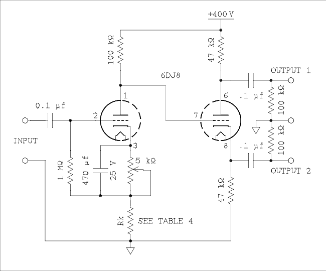
Figure 4 6DJ8 Inverter/Driver.
For a verbal description click here.
Now the Data Table. All tests were performed with 1.00 volts input.
Table 4
6DJ8 Inverter/Driver With Cathode Degeneration.# Rk in
Amplifier
(kΩ)Overall
GainVk SLPI
For Min
THD (V)THD (%)
Vin = 1 V
Plate/Cathode1 4.7 11.3 152 ~0.065/0.085 2 4.7 10.3 159 ~0.060/0.077 3 4.7 10.4 160 ~0.054/0.072 4 4.7 10.4 156 ~0.101/0.121 1 2.2 16.9 148 ~0.184/0.204 2 1.5 17.0 152 0.235/0.255 3 1.5 17.1 152 ~0.207/0.227 4 1.2 17.3 152 0.370/0.390 ~ Both values corrected for distortion in signal source.
When Rk = 4.7 k ohms the gain given by LT Spice is 11.34.
With 2.2 k, gain is 16.52.
With 1.8 k, gain is 17.83.
With 1.5 k, gain is 18.95.
With 1.2 k, gain is 20.22.You can see in the chart above that there was considerable variation among real tubes. The LT Spice simulation only has one version of each tube and the numbers above tell the story. Probably an RK of 5.6 k would have given a gain much closer to 10 or 10.6 which is the actual gain needed but if you want to know you will have to download your own version of spice and do it for yourself.
The data in table 4 shows that a gain of 10 with low distortion can be easily achieved. This would be a zero GNFB amplifier using 6V6s. This tube type produces more distortion than the others listed in the table. It may be possible to lower the distortion using some form of local feedback but that remains to be seen. The 17 volt level allows the use of type 6L6 and 6550. The latter gives quite low distortion when operated at the less than maximum power of 55 watts. You might get a tolerable sounding zero GNFB amplifier if you don't push it to full power, say 20 watts.
Wise Bootstrapped Amplifier with SLPI Inverter.
We can't get the gain of 25 with the circuit of figure 4 so we will have to try figure 5. This is a bootstrapped plate load circuit. Bootstrapping the plate load increases the gain of an amplifier by making the effective AC resistance of the plate load very high, in the meg ohm range. The plate load resistor has been replaced by two resistors. The lower one is the plate load and the other one is the resistor that permits the bootstrapping voltage to be applied to the upper end of the plate load. The bootstrapping voltage is in phase with the plate voltage of the amplifier so both ends of the load resistor go up and down together. They are not quite together because the SLPI has a gain of slightly less than unity. This is a good thing because it keeps the circuit from oscillating.Circuits of this kind you have probably seen before make the cathode resistor of the SLPI equal to the bootstrapping resistor. Then the plate resistor is cut in half to balance the circuit. The arrangement shown in figure 5 comes from a design by John Wise. The traditional circuit is balanced for AC but not for DC. The SLPI plate and cathode resistors remain unchanged. The bootstrapping resistor is 100 k ohms. It is AC coupled to the cathode of the SLPI by a 1 microfarad capacitor. Then to maintain AC balance another (dummy load) 100 k ohm resistor is AC coupled to the plate by another 1 uf capacitor. This has the effect of maintaining both AC and DC balance on the SLPI. So why is the dummy resistor 120 k ohms? It is most likely due to the difference in output impedance between the plate and cathode. When I Breadboarded the circuit there was a considerable imbalance between the plate and cathode outputs with the plate being low. Replacing the 100 k ohm with a 120 k ohm resistor brought it back into balance within 1%. I have never seen this circuit arrangement before. John should receive credit for coming up with it.
Figure 5 The Wise Version of a Bootstrapped Amplifier.
For a verbal description click here.
Table 5
6DJ8 Inverter/Driver With Bootstrapping.# Overall
GainTHD (%) @ 10 V
Plate/CathodeTHD (%) @ 17 V
Plate/CathodeTHD (%) @ 25 V
Plate/Cathode1 31 ~0.051/0.038 ~0.082/0.037 ~0.115/0.060 2 25.4 ~0.025/TSM ~0.031/TSM ~0.049/0.017 3 25.8 ~0.089/0.053 ~0.143/0.094 ~0.213/0.158 4 25.5 ~TSM/0.047 ~0.014/0.086 ~0.040/0.130 Bootstrapping the amplifier will yield a gain almost equal to the amplification factor. The tube manual value of amplification factor is 33. Tube 1 is a Tung Sol and is likely American made NOS. Looking back to table 2, tube 1 when used as an SLPI gave a gain of 0.942. If we divide the amplifier gain by the SLPI gain we get 32.9. Close enough? The other three tubes look as though the labeling was painted by a child using a brush that was too big for the job. You would think that a manufacturer would be ashamed to let a product that looks like that out the door. Nobody has pride in workmanship anymore. Just get it out the door and make the money. End of rant.
The tubes that were made on mars, or wherever, did give us a desired gain figure of 25. We have shown that using the 6DJ8 as the preinverter amplifier and the SLPI can be made to yield a gain of 10, 17, or 25. Also a gain of approximately 33 with the right tube. But this severely limits the choice of output tubes and amounts of GNFB. However, it is possible to use another dual triode to complete the Williamson circuit and use the gain adjusting techniques below to obtain the desired gain for a particular set of power tubes and amount of feedback.
With one exception the values in the schematic give a spice gain of 28.7. That one exception is the 120 k ohm resistor that is capacitively coupled to the 47 k ohm in the plate of the SLPI. In the spice simulation it had to be 107.5 k ohms to achieve balance between the two outputs. The resistor taking the place of the rheostat is 2.4 k ohms. The gain is very close to being halfway between 25 and 33 which could make it a useful compromise value. Spice tells me the same thing I found on the breadboard that increasing the value of Rk has almost no effect on the gain and increases the amount of distortion. That's somewhat reassuring.
Although for most values of gain the distortion was low enough to be used in a zero GNFB amplifier I think the best bet is to use only one 6DJ8, one section per channel. With that in mind we will now examine a variety of tube types as the preinverter amplifier and adjust the gain with local feedback.
Applying local negative feedback around the amplifier - SLPI combination.
This concept is not new with me. At one time I had a circuit in which local NFB was placed around an SLPI posted on the phase inverter page of the how amplifiers work section of this site. I took it down because it did not fit in with the educational aspect of that section. I don't recall ever having seen this method in any of the electronics literature or in commercially produced audio amplifiers. I think it could be used as an effective strategy for lowering distortion without increasing the tube count.The gain of a bootstrapped amplifier can be changed in only one way that I know of. That is by applying NFB around it. I ask you to compare figures 5 and 6. The upper end of the 120 k ohm dummy load resistor has been lifted from the B+ line and connected to the junction of the 100 ohm resistor and the 5 k ohm pot (rheostat). Note: it could be connected directly to the cathode or where it is shown. The 470 uf capacitor makes these two points the same for AC. The difference in DC potential makes no difference because of the 1 uf capacitor connected to the other end of the resistor. Also you will note that the value of the resistor has been changed from 120 k ohms to 330 k ohms. Note also that the value of the bootstrapping resistor has been changed from 100 k ohms to 270 k ohms. The value of Rk has also been changed. It is no longer 100 ohms. Its resistance sets the value of B* which sets the gain of the amplifier gain to the desired value. The negative feedback path is from the plate of the SLPI to the cathode of the preinverter amplifier.
* Gain is determined by the equation A' = A / (1 + AB). A = gain without feedback, A' = gain with feedback, and B = fraction of output signal fed back.
I can't come up with any other way of altering the gain of a bootstrapped amplifier. I tried AC coupling a load resistor to the plate of the amplifier which did reduce the gain but it also increased the distortion by a large amount. Cathode degeneration will only decrease the gain by a miniscule amount. But it does greatly increase the distortion. Bootstrapping turns the tube into a constant current device. There is no, or a very small, AC component of cathode current to produce degeneration.
Yet another digression. GNFB and a Bootstrapped Amplifier.
There is a question in my mind as to whether GNFB can be applied to the cathode of a bootstrapped amplifier. Let's look at the theory and then make some measurements on the breadboard.To make the numbers easy let's assume an amplifier with 20 dB of GNFB. We will inject a signal of 1 volt and the voltage at each output of the phase inverter will be 25 volts. It doesn't matter whether the output tubes are 6L6GCs, EL34s or 6550s. In a correctly designed amplifier the gain of the power tubes, the turns ratio of the output transformer and the value of the feedback resistors have all been worked out so the above is true.
So we connect our AC voltmeter to the grid of the bootstrapped amplifier and it reads 1.00 volts. At the grid of each power tube it reads 25.0 volts. At the cathode of the bootstrapped amplifier it reads 0.90 volts. That's because 20 dB of GNFB reduces the gain by a factor of 10. With the GNFB disconnected it would only take 0.10 volts to produce 25 volts at each power tube grid. With GNFB disconnected there is no AC voltage at the cathode of the Bootstrapped amplifier. So as long as there is 0.10 volts between the cathode and grid of the amplifier the output of the phase inverter will produce 25 volts at each output.
If we were to use a dual output function generator to introduce two sine wave signals, one of 1.00 volts at the grid and the other of 0.90 volts at the cathode the output of the phase inverter would be 25 volts.
Our Breadboarded circuit delivers 25.4 volts with an input to the grid of 1 volt. The resistor in the cathode is a 100 ohm so I applied output 2 of my FG across it and output 1 set 1 volt higher than output 1 to the grid. With 4 volts on the grid and 3 volts on the cathode the output was just a little low. I had to decrease the voltage applied to the cathode to obtain 25.4 volts. The difference was 1.114 volts. At these settings the distortion figures were 0.069 on the output plate and 0.057 on the output cathode. The variation from 1 volt is not especially significant. Negative feedback will correct for the errors and make it come out right. Well OK, the actual closed loop gain will be a little off from the calculated value but you'll never hear the difference.
Conclusion. GNFB will work normally when applied to the cathode of a bootstrapped amplifier.
End of Another Digression.
Nine Circuits Using Preinverter Amplifier and SLPI.
In spite of Pandora's claims of wisdom acquired while living a long time she Is not at all acquainted with the internet and states emphatically that she has no desire to become so. Her suggestion of 9 separate schematic diagrams makes a large webpage even larger. As I worked out the circuits and made measurements on them they fell into 3 groups of 3 each. Gains of 10, 17, and 25 using a 12AY7, with the only difference between the three being the value of one resistor. Gains of 33, 50, and 75 used a 12 AX7 and it looked exactly like the first three except for the label on the tube symbol. Gains of 100, 170, and 250 required a pentode but still all three were the same except for one resistor. All of this information can be presented in two diagrams and one table.
Table 6
Gain Values for Preinverter Amplifier and 6DJ8 Inverter.Overall
GainPreinverter
Amplifier
TubeRk (Ohms)
Figure 6 &
Figure 7Recommended
Vo (VAC)Suggested
GNFB (dB)10 1/2 12AY7 16 k 10 0 17 1/2 12AY7 7.5 k 17 0 25 1/2 12AY7 2.7 k 25 0 33 1/2 12AX7 4.7 k 10 10 50 1/2 12AX7 2.2 k 17 10 75 1/2 12AX7 680 25 10 105 6BH6 2.2 k 10 20 165 6BH6 1.3 k 17 20 250 6BH6 820 25 20 The conditions on the lines that give gains of 10, 33, and 105 in table 6 are suitable for use in an amplifier with type 6V6, 6AQ5, or other output tube types that require approximately 10 volts RMS per tube. With the exception of an amplifier with 20 dB of GNFB, these tubes must have some kind of distortion reducing local feedback or other tricks to reduce distortion. If I ever finish this project I'm going to do another one on reducing distortion in power output tubes.
One rather unorthodox trick might be to use a more powerful tube such as a 6L6 or EL34 but hide the real amplifier and build a dummy amplifier with 6V6s. Then tell all your friends that it is a 15 watt per channel amplifier. Evil grin.
The conditions on the lines that give gains of 17, and 50, in table 6 are suitable for use in an amplifier with type 6L6G/GT, 6550, or other types that require approximately 17 volts RMS per tube. With the exception of an amplifier with 20 dB of GNFB or amplifiers with type 6550, these output tubes must have some kind of distortion reducing local feedback or other tricks to reduce distortion.
The conditions on the line that gives a gain of 25 in table 6 is marginal for use in an amplifier with 0 dB of GNFB. I don't recommend its use.
The gain of 75 line in table 6 is just barely suitable for use in an amplifier with 10 dB of GNFB. This amount of feedback should reduce the distortion by an approximate factor of 3. You could use this value of gain if you have distortion measuring equipment to select the best tube out of several. Otherwise I do not recommend its use.
The conditions on the lines that give gains of 165 and 250 in table 6 are not suitable for use in any amplifier. It makes more sense to use the full Williamson circuit for these combinations of gain and output level. However, these are intended for use inside a 20 dB GNFB loop. They still might be used if a low bottle count is one of the design goals.
This seemingly useless data has been provided for the sake of completeness and on the chance that someone may get a good idea from studying the circuitry.
Figure 6 Triode Amplifier and 6DJ8 SLPI.
For a verbal description click here.
The reader should be constantly aware that in all 9 tables below, 6A through 6J, the SLPI is 1/2 of a 6DJ8.
An additional line will be appended to each table below giving the LT Spice results. The cathode voltage will be set to the average of the four values for the real tubes in the table.
12AY7
Tube 1 is in a GE box but the tube itself has only the number 6072A and below Made in USA.
Tube 2 is in a military box, has the GE logo, and made in USA on the tube.
Tube 3 is identical to tube 1.
Tube 4 is identical to tube 2.1. Gain of 10.5, 10.5 Volts Output With 12AY7.
Table 6-A
12AY7 Amplifier with Rk = 16 k Ω.# Overall
GainVk for
min THD (%)THD (%) @ 10.6 V
Plate/Cathode1 10.6 139 TSM/TSM 2 10.9 133 TSM/TSM 3 10.9 135 TSM/TSM 4 10.6 133 TSM/TSM LTS 11.54 135 0.1607/0.1628 2. Gain of 17, 17 Volts Output With 12AY7.
Table 6-B
12AY7 Amplifier with Rk = 7.5 k Ω.# Overall
GainVk for
min THD (%)THD (%) @ 17 V
Plate/Cathode1 17.0 150 ~TSM/0.033 2 17.5 142 ~TSM/0.047 3 17.0 152 ~0.025/0.015 4 17.0 148 ~0.020/0.021 LTS 17.59 148 0.2973/0.3003 3. Gain of 25, 25 Volts Output With 12AY7.
Table 6-C
12AY7 Amplifier with Rk = 2.7 k Ω.# Overall
GainVk for
min THD V)THD (%) @ 25 V
Plate/Cathode1 25.6 140 ~0.190/0.243 2 26.5 140 ~0.145/0.195 3 25.3 140 ~0.205/0.153 4 25.2 140 ~0.189/0.138 LTS 25.83 140 0.7029/0.7080 12AX7
Tube 1 is a Sylvania. Both the box and tube are labeled 12AX7A-ECC83-7025.
Tubes 2 and 3 are in tan boxes which at one time were probably white. They have those long military procurement numbers printed on the side. Tube 2 is a CBS and 3 is a Sylvania. On both tubes the number is preceded by the letters JAN which stands for joint army navy not the first month of the year.
Tube 4 is a GE tube in an RCA box.
4. Gain of 33, 10 Volts Output With 12AX7.
Table 6-D
12AX7 Amplifier with Rk = 4.7 k Ω.# Overall
GainVk for
min THD (%)THD (%) @ 10.6 V
Plate/Cathode1 34.4 138 ~TSM/0.039 2 33.4 138 ~0.057/0.017 3 34.1 158 ~0.038/0.077 4 32.2 119 ~0.046/0.045 LTS 34.55 138 0.1330/0.1348 5. Gain of 50, 17 Volts Output With 12AX7.
Table 6-E
12AX7 Amplifier with Rk = 2.2 k Ω.# Overall
GainVk for
min THD (%)THD (%) @ 17 V
Plate/Cathode1 52.6 149 ~0.031/0.012 2 50.0 137 ~TSM/0.049 3 52.9 149 ~0.369/0.394 4 47.8 116 ~0.195/0.178 LTS 50.75 137 0.2679/0.2709 6. Gain of 75, 25 Volts Output With 12AX7.
Table 6-F
12AX7 Amplifier with Rk = 680 Ω.# Overall
GainVk for
min THD (%)THD (%) @ 25 V
Plate/Cathode1 75.8 134 ~0.171/0.183 2 71.4 139 ~0.054/0.061 3 78.1 141 0.98/0.94 4 66.7 120 0.46/0.48 LTS 71.72 134 0.5572/0.5619 7. Gain of 105, 10.5 Volts Output With 6BH6.
Figure 7 Pentode Amplifier and 6DJ8 SLPI.
For a verbal description click here.
6BH6
Tube 1 is a Tung Sol in a well warn box.
Tube 2 is not decipherable and came in a new white box.
Tube 3 is a GE in a well warn box.
Tube 4 has the number printed over other printing. It came in a new Motorola box.
Make of that what you can.The 6BH6 is the tube that is being changed.
Table 6-G
6BH6 Amplifier with Rk = 2.2 k Ω.# Overall
GainVk for
min THD (%)THD (%) @ 10.6 V
Plate/Cathode1 105 112 ~0.136/0.189 2 100 115 ~0.160/0.103 3 104 114 ~0.162/0.108 4 103 111 ~0.122/0.079 LTS 113.8 113 0.2381/0.2353 8. Gain of 165, 17 Volts Output With 6BH6.
Table 6-H
6BH6 Amplifier with Rk = 1.3 k Ω# Overall
GainVk for
min THD (%)THD (%) @ 17 V
Plate/Cathode1 167 113 ~0.400/0.301 2 155 120 ~0.389/0.295 3 165 109 ~0.349/0.264 4 165 112 ~0.269/0.189 LTS 18.23 113.5 0.5775/0.5729 9. Gain of 240, 25 Volts Output With 6BH6.
Table 6-J
6BH6 Amplifier with Rk = 820 Ω.# Overall
GainVk for
min THD (%)THD (%) @ 25 V
Plate/Cathode1 238 144 0.715/0.880 2 210 140 1.05/0.91 3 240 118 0.810/0.645 4 238 112 0.655/0.515 LTS 26.63 128.5 0.8805/0.8746 The 6BH6 model wasn't good enough to work in the simulation so the 6AU6 model had to be used instead. In truth I don't think there is very much difference between the real tubes.
Summary of SLPI and Preinverter Amplifier Only.
If you are looking to build a zero GNFB amplifier the gains of 10 and 17 look very good but you may have some difficulty finding suitable output tubes for the gain of 10. The gain of 25 setting seems to have too much distortion for such an amplifier.The gain of 50 seems especially appealing for a 10 dB GNFB amplifier with 6550s. A gain of 33 less so for reasons cited above. The gain of 75 can be useful if you have distortion measuring equipment to select tubes. The large appeal of these three gains is, they place only one low frequency RC roll off in the feedback loop.
Gains of 100, 165, and 250 are intended for use in a 20 dB GNFB amplifier. Their use may not be as appealing because they have two low frequency RC roll offs. The screen grid bypass adds one more.
Building up to the full Williamson circuit.
The postinverter amplifier.
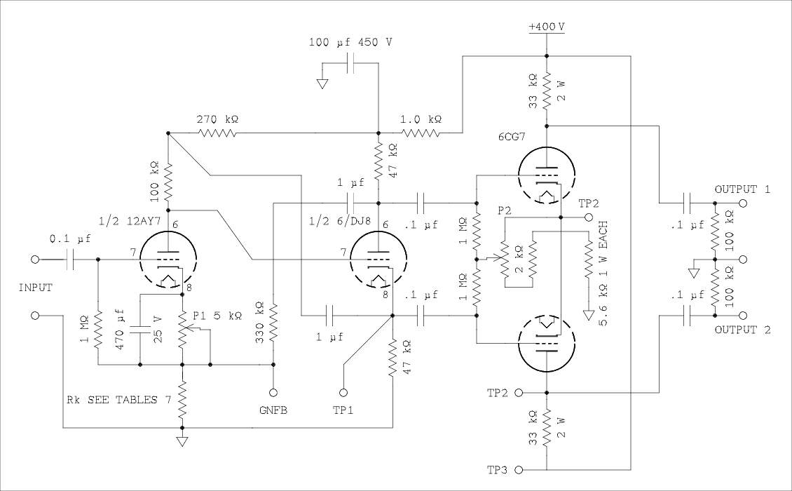
Figure 8 Williamson Circuit Less Power Outputs.
Adjust P1 for anything from 100 to 140 volts DC at TP1.
Adjust P2 for 125 volts DC at TP2.
For a verbal description click here.
Table 7
Williamson Circuit with Resistor in Cathodes of Postinverter Amplifier.Figure 8 Rk = 16 k ohms. Vo = 17 VAC. Figure 8 Rk = 9.1 k ohms. Vo = 25 VAC. Tube Gain THD
P1/P2IMD
P1/P2f2 (kHz) Tube Gain THD
P1/P2IMD
P1/P2f2 (kHz) 1 180 0.069/0.069 0.275/0.260 71 1 255 0.123/0.106 0.400/0.365 71 2 181 0.043/0.119 0.245/0.360 70 2 256 0.134/0.086 0.30/0.41 74 3 173 0.071/0.080 0.255/0.250 63 3 245 0.105/0.086 0.35/0.23 74 4 180 0.069/0.068 0.260/0.380 63 4 243 0.158/0.136 0.37/0.48 74 Remembering that these two gain values are intended for use inside a GNFB (global negative feedback) loop the distortion values aren't out of line. It should be possible to build a pretty respectable amplifier using this circuit with many popular output tube types.
Now let's see what effect a current sink in the cathodes will have. As shown below. Hmmm, looks a lot like a long tail pair, doesn't it.
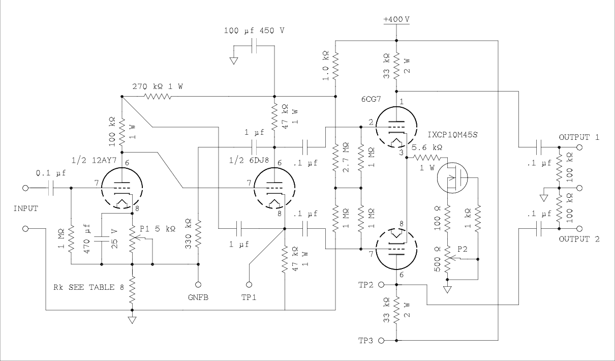
Figure 9 Williamson Circuit With Current Sink in Cathodes of Postinverter Amplifier.
Adjust P1 for 120 VDC at TP1
Adjust P2 for 170 VDC between TP2 and TP3.
For a verbal description click here.
Table 8
Williamson Topology with current sink in cathodes of Postinverter Amplifier.Figure 9 Rk = 16 k ohms. Vo = 17 VAC. Figure 9 Rk = 9.1 k ohms. Vo = 25 VAC. Tube Gain THD
P1/P2IMD
P1/P2f2 (kHz) Tube Gain THD
P1/P2IMD
P1/P2f2 (kHz) 1 178 0.055/0.052 0.245/0.245 65 1 252 0.101/0.102 0.385/0.385 74 2 180 0.047/0.045 0.210/0.195 64 2 256 0.078/0.074 0.285/0.275 75 3 170 0.029/0.028 0.190/0.185 64 3 242 0.055/0.056 0.22/0.23 74 4 167 0.079/0.081 0.31/0.30 64 4 238 0.127/0.125 0.44/0.43 74 * For IMD measurements the output voltage used was 80% of the stated value.
Well. That looks surprisingly good. Even the recalcitrant tube 4 gave acceptable results. However the ratios of IMD to THD hovered between 4 and 5 which is not what I was hoping for. Nonetheless In my opinion the current sink in the cathodes is worth the extra parts especially when they are so inexpensive compared to the price of the tubes. However I could wish for a higher -3 dB frequency. I don't know yet if there is anything I can do about that.
There is a loose end that needs to be tied up. We have low distortion with gains of 170 and 250 but what about those gains of 25, 50, 75, and 100, that we rejected in the earlier circuit. And while we are doing all of those we might as well throw in the gain of 33 for free.You no doubt have noticed that in all 8 schematic diagrams above there is not so much as one grid stopping resistor. I believe this to be a solution in search of a problem. There is one notable exception which is a pentode output stage. These circuits have all the ingredients to produce parasitic oscillation. These are; relative high impedance in the grid circuit, high gain, and the presents of inductance in the plate circuit. Power output tubes don't always oscillate or even ring but the chances of it happening are greater than zero. On the other hand a triode amplifier with no inductance in the circuit is not at all likely to oscillate. I would say to those who like them, if they make you feel good use them. But keep in mind that resistance in series with the signal path can combine with stray and Miller capacitance to form a low pass filter and reduce the high frequency limit of the circuit. This can make an amplifier with GNFB more difficult to compensate for stability.
Table 9
Williamson Topology Adapted for lower gain values.
1/2 12AU7 As Preinverter Amplifier.Conditions Tube 1 Tube 2 Tube 3 Tube 4 Rk
(k Ω)P1
(k Ω)Vo
(VAC)Gain THD (%) Gain THD (%) Gain THD (%) Gain THD (%) 18 10 10.5 103 0.032/0.034 105 0.029/0.033 100 0.031/0.033 97 0.030/0.033 33 10 25 75 0.063/0.062 72.7 0.065/0.064 72.1 0.066/0.066 70.3 0.061/0.061 56 10 17 52.6 0.038/0.038 50.9 0.038/0.038 50.6 0.36/0.37 49.7 0.36/0.36 100 5 10.5 34.4 0.046/0.039 34.1 0.048/0.043 35.0 0.048/0.043 33.8 0.044/0.038 100 5 25 34.4 0.098/0.105 34.1 0.089/0.096 35.0 0.084/0.088 33.8 0.100/0.105 Table 9 above shows excellent results. You are probably wondering what's with the last line of the table. I couldn't get the gain down to 25 without increasing the distortion to unacceptable levels. If you use these conditions in a zero GNFB amplifier as suggested in table 6 the input for full power will be about 0.7 volts which once was the standard. The values given for Rk and P1 refer to figure 9 except that the triode on the left is 1/2 12AU7.
Adding Frequency compensation.
Earlier I noted that I had tried to reduce the gain of the bootstrapped amplifier by capacitively coupling a resistor to the plate. Because this seriously increased the distortion I became worried about the effect of the familiar series RC circuit that is almost universally used to compensate the feedback loop so it will not oscillate or ring on transients. So I connected one with typical values and tested the distortion over the upper audio band, from 1 kHz to 20 kHz.
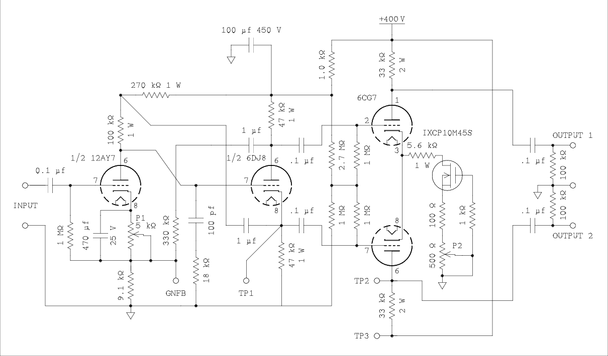
Figure 9-A Williamson Circuit With Frequency Compensation on Plate of Preinverter Amplifier.
For a verbal description click here.
I tested it under pessimistic conditions. The cathode resistor is set for minimum local NFB, the compensating resistor is lower than typical, and the capacitor value higher. The output resistance at the plate of the 12AY7 is about 180 k ohms. The gain starts rolling off at about 7.5 kHz. The compensation network flattens out at around 75 kHz where the amplifier begins its natural roll off. I measured the distortion at 1, 2, 5, 10, 15, and 20 kHz. The value hung right around 0.05% +/- 0.002% for all frequencies except 20 kHz. At that frequency it measured about 0.075%. Clearly we have nothing to worry about.
Summary of Williamson Inverter Driver.
I recently received an email message from someone who stated that he wished the "bottle count" in audio amplifiers could be reduced. If you are similarly inclined you may be attracted to the circuit above that uses only two triodes. Some of them I would use and some I wouldn't. You will have to evaluate the data and make your own decision.Meanwhile the full Williamson circuit gives excellent low distortion and gain control for different amplifier designs. Indeed the resistor labeled as RK in figure 9 could be changed to a rheostat connected potentiometer and the gain adjusted to suit the tubes that are in the sockets. A 25 turn pot is highly recommended because at some settings a 1 turn pot could be difficult to adjust.
There must be thousands of amplifier circuits and some have more tubes than others. The person who sent me that email message will not be pleased with where we are going next.
Someone on the list had suggested that I try some 6N6P Russian tubes. They appear to be comparable to the 6CG7 so before tearing down the breadboard I decided to try a few, I have 10. They gave a bit more distortion than the CGs and the amounts were not as closely matched between the two sections. In keeping with previous data gathering I tried 4 of them. The best was comparable to the best of the 6CG7s. The worst gave 5 times the distortion of the worst 6CG7. They might have some use but it does not appear to be in low distortion audio amplifiers.
Some Lessons Learned From Analyzing the John Wise circuit, Below.
In the analysis of the John Wise circuit which you haven't read yet we learned that the first triode of a Williamson circuit operates at such a low level that bootstrapping it amounts to gilding the lily. If the first two triodes were to be used alone the circuit clearly would benefit from bootstrapping. There seems to be a lesson in that for my version of the Williamson circuit. After some false starts I came up with the circuit of 9-B below.
Figure 9-B Idealist's Williamson Circuit.
For a verbal description click here.
This is the ideal circuit. The series combination of the 1 uf capacitor and 100 k ohm resistor in the cathode of the second triode balances the 1 uf capacitor and 100 k ohm feedback resistor connected to the plate. The DC part of the circuit is also balanced by the two 47 k ohm resistors.
Then I did a mad man Munts on it. For those who may not be familiar with Munts TV sets and its eccentric owner, the legend is that he would walk through the development labs with a pair of diagonal cutters in hand, clipping out components in the prototypes. If the set continued to work he would order the engineers to leave that part out of the design. True or false? I don't know but it is a good story. I took out parts I thought it might do without. The circuit of figure 9-C works just as well as the one of figure 9B. If you are a purest you will probably use figure 9-B. If you want minimum complexity use the circuit of figure 9-C. I haven't decided which one I would use.
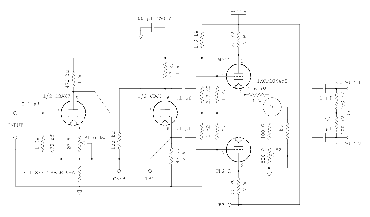
Figure 9-C Minimalist's Williamson Circuit.
For a verbal description click here.
Table 9-A
Williamson circuit Without Bootstrapping.
1/2 12AX7 As Preinverter Amplifier.Gain Rk1 (kΩ) Vk2 (VDC) Vo (VAC) THD (%)
O1/O2f2 (kHz) 245 4.7 120 24.5 0.135/0.132 140 170 7.5 130 17.0 0.076/0.074 137 98 15 135 9.8 0.040/0.044 135 72 22 135 25 0.148/0.146 136 52 33 147 17 0.078/0.078 141 As you can see the performance is quite respectable. Remember that all of these gain values are intended to go inside of a global negative feedback loop.
Someone has already pointed out to me that the distortion inherent in output tubes is much higher than that measured in these phase inverter circuits. I am sure I measured distortion in a pair of 6550s that were being driven by a very low distortion inverter circuit that was well below 0.5%. Unfortunately I didn't document the measurement so I need to go back and measure it again. I guess my next project will be to examine various output tubes to see if there is anything that can be done to reduce their distortion. Meanwhile, have fun.
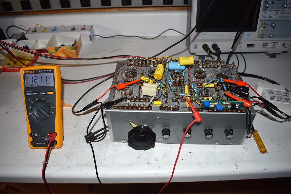
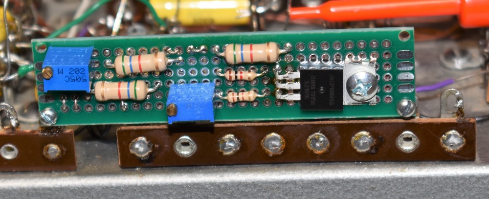
A Look At the Breadboard.
For a verbal description click here.
This solder breadboard was made of a recycled half of a Bud box. The largest that Bud made. As you can see it uses lots of terminal strips and tube sockets. It provides a ground plane almost as good as a regular chassis. Because I had to change Rk so often I used two of the modular connectors from the old DeVry system to make the job a lot quicker. The transistor and tiny pots were mounted on a small circuit board. This was the smallest one of an assortment of different sizes that are all over eBay and Amazon. The bottom picture is a close up of the board. The cathode circuits for figures 8 and 9 were both assembled on the board. When I build an amplifier that incorporates this hybrid technology I will certainly use this same technique. The board has holes at the 4 corners. I inserted two, 2-56 screws through the holes at two corners, threaded a nut on each, pushed the ends of the screws through the openings in terminal strip lugs, and installed another nut on each screw. This gave me a sturdy platform for adjusting the pots.
The Wise Linearized Williamson Amplifier.
John Wise and I have been exchanging email messages for several years. His approach to phase inverter design is presented here. he starts with the Williamson design and makes changes to improve its performance. As I have done previously, I will begin with the preinverter amplifier and SLPI without bootstrapping but with resistors and capacitors in strategic places designed to minimize the effect of changes that add the bootstrapping. Then I will build up to the circuit as he designed it. I may or may not suggest changes. At this writing the breadboarding and measurements are yet to be done.
Figure 10 Preinverter Amplifier and SLPI With Bootstrapping Removed.
For a verbal description click here.
One feature of John's design is the use of electrolytic capacitors for coupling. To avoid the real or imagined effect of electrolytic capacitors at high audio frequencies each 10 uf electrolytic has a 0.033 uf plastic film capacitor connected in parallel with it. To unclutter the schematic I have shown each of these as a single capacitor marked with a *. I will investigate this effect while I have the chance.
I wish to measure the effect of bootstrapping. Figure 11, below, shows the preinverter amplifier and SLPI portion of John's circuit. Figure 10, above shows how I have gone about removing it. The reader is encouraged to compare the two circuits. First of all when the coupling capacitor is disconnected from the cathode, pin 6, it can't be left hanging. The cathode is a very low impedance point so the disconnected end is connected to ground. Otherwise the plate of the amplifier triode would see a plate load of 136 k ohms instead of 68 k ohms. Disconnecting the bootstrapping capacitor from the cathode leaves it with a load of 68 k ohms instead of the 34 k it sees when the bootstrapping is connected. Therefore I need to capacitively couple another 68 k ohm resistor to the cathode to keep things in balance. Note that John has called for a capacitively coupled load in the plate circuit.
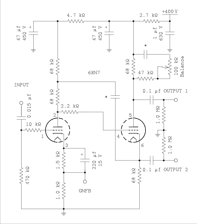
Figure 11 Preinverter Amplifier and SLPI With Bootstrapping.
For a verbal description click here.
Let's collect some data on this circuit. For each distortion test I set the output level to 1.5 volts to be consistent with the data above. For the high end corner frequency (f2) I set the mid band output to 1.50 VRMS as indicated by the measurement on the scope screen and cranked up the frequency until the display read 1.06 volts.
Tube 1 is a Raytheon. It stands 2-5/8" above the chassis. Like other Raytheons the box appears newer than other tubes.
Tube 2 is a Magnavox in an RCA box. It stands 2-5/16".
Tubes 3 and 4 are Sylvania and stand 2-3/16" high.
Without bootstrapping the balance pot needed to be adjusted only once. After bootstrapping was connected it had to be adjusted for each tube.
Table 10
Gain and Distortion of an Amplifier / SLPI Combination.No Bootstrapping Figure 10 Bootstrapped Figure 11 # Gain THD (%)
P/KIMD (%)
P/Kf2 (kHz) Gain THD (%)
P/KIMD (%)
P/Kf2 (kHz) 1 11.5 0.036/0.056 0.195/0.190 133 16.4 0.032/TSM 0.048/0.029 93 [230] 2 10.4 0.042/0.060 0.218/0.202 143 14.7 0.0685/0.0295 0.175/0.109 102 [260] 3 11.1 0.076/0.094 0.340/0.340 155 15.8 TSM/TSM 0.015/0.043 110 [280] 4 11.5 0.088/0.105 0.380/0.380 156 16.3 TSM/0.0295 0.033/0.066 111 [285] This paragraph was written after taking the THD without bootstrapping. Now that does look suspicious, doesn't it. Each tube has a higher distortion than the one before it. A viewer of this page would be likely to conclude that I had equipment drift. So before the setup was changed I went back to tube 1. It gave figures of 0.037 and 0.057. A very small amount of drift but well within the specifications of the instruments. The tubes were chosen at random from my stock without benefit of any pretesting.
Above I expressed a dislike for grid stopping resistors. Now I have evidence to back up my opinion. The figures in brackets [ ] were taken with the 10 k ohm and 2.2 k ohm grid stopping resistors, shown in the diagram, removed. The cause is the resistor in conjunction with the Miller capacitance of the amplifier stage. The capacitance that is multiplied by the gain + 1 is more than the plate to grid capacitance of the tube. It is that plus the capacitance between the plate circuit wiring and grid circuit wiring. It doesn't take much wiring to make 5 pf of capacitance. The section that connects to pins 1,2, and 3,* has a plate to grid capacitance of 3.8 pf so 8.8 pf times 16 gives 141 pf. When combined with a 10 k ohm resistor the corner frequency is 113 kHz. That's not bad considering that it is based on an estimate of the wiring capacitance. Earlier I stated that the grid stopping resistor was a solution looking for a problem. I wish to change that. The grid stopping resistor is a problem looking for a solution. In this cased the solution is obvious. Take the damned thing out.
* In the Sylvania tube manual the section connected to pins 1, 2, and 3, is section 2. I wonder what bright clever young engineer came up with that one.
Figure 12 Pre and Postinverter Amplifiers and SLPI With Post Amplifier Bootstrapping Removed.
For a verbal description click here.
Figure 13 Pre and Postinverter Amplifiers and SLPI With Post Amplifier Bootstrapping.
For a verbal description click here.
V1 = tube 2.
V2 = tube to be changed.
V3 = tube 1.
The input level was set at 0.10 volts and not changed. This placed the output of the SLPI at 1.50 VAC and the output at the cathodes of V3 at approximately 19 volts. Divide the gain by 0.1 to learn the output voltage. The balance control was adjusted for the first tube and not changed. Balance varied by about +/- 2%.
Table 11
Gain and Distortion of the Full Williamson Circuit.Without Bootstrapping Figure 12 Bootstrapped Figure 13 # Gain THD (%)
O1/O2IMD (%)
O1/O2f2 (kHz) Gain THD (%)
O1/O2IMD (%)
O1/O2f2 (kHz) 3 192 0.62/0.68 1.71/2.07 171 242 0.123/0.057 0.255/0.196 162 4 178 0.43/1.5 1.15/4.60 165 235 0.108/0.245 0.32/0.61 155 5 177 0.36/0.94 1.00/2.85 163 235 0.140/TSM 0.158/0.440 147 6 195 0.29/1.3 0.895/4.00 165 252 0.096/0.054 0.335/0.149 148 This is my reaction after collecting gain and THD data for the Williamson circuit without bootstrapping. "Well, that doesn't seem so hot, does it." I might as well forge on ahead and take the IMD data. IMD follows the trends of THD. Now for the frequency data. Then I'll connect the bootstrapping to see how much of an effect it has.
For this part of the test I adjusted the balance for equal output voltage for each tube. I had not done this before.
Now I need to see how different tubes plugged into socket V3 effect the performance. Tube 3 is in socket V2.
Table 12
Gain and Distortion Results
From Changing V3 Figure 13.# Gain THD 1 242 0.128/0.068 4 245 0.188/0.119 5 243 0.242/0.210 6 244 0.130/0.110 Electrolytic Capacitors in the Signal path.
What about the commonly heard and red opinion that electrolytic capacitors when placed in the signal path introduce problems at high audio frequencies. John has specified a common cure which is to connect smaller film capacitors in parallel with electrolytics. The bootstrapping coupling capacitors are 10 uf electrolytics each with a 0.033 uf film capacitor in parallel. Let's collect some performance data and then remove the film caps to see what happens.
Table 13
Gain and Distortion Results From Removing Film Capacitors From Electrolytics.Film & Electrolytic in Parallel Electrolytic Only Vo = 25 VAC Vo = 2.5 VAC Vo = 25 VAC Vo = 2.5 VAC Frequency
(kHz)Gain THD (%)
O1/O2Gain THD (%)
O1/O2Gain THD (%)
O1/O2Gain THD (%)
O1/O21.0 243 0.13/0.063 240 0.061/0.062 242 0.128/0.066 240 0.058/0.058 10 243 0.14/0.093 243 0.090/0.081 243 0.125/0.068 240 0.09/0.079 20 243 0.13/0.082 243 0.090/0.081 240 0.14/0.075 240 0.09/0.081 40 238* 0.19/0.086 238* 0.086/0.081 240* 0.195/0.068 238* 0.085/0.079 * About 1% imbalance.
Poof! There goes another myth up in smoke. Looks like some of the distortion readings are higher and some are lower. Unfortunately I was not able to take data for both conditions in one unbroken run. A doctor's appointment got in the way and I didn't have time. Between "with film caps" and "without film caps" There was a 3 hour cooldown period. But I think it is safe to say that the differences are not statistically significant.
Summing Up So Far.
This circuit performs nicely when it is complete. Testing in pieces revealed some really bum tubes but the circuitry overcame them and showed generally good performance.Most of my stock of 6SN7s consists of military surplus tubes in tan boxes with those long military procurement numbers printed on the side. I pulled out 3 different tubes at random and installed them in the sockets. The performance was quite good. Gain of 257, and THD of 0.115% from output 1, and 0.148% from output 2. This falls within my desired goal of less than 0.15%.
The performance of the preinverter amplifier and SLPI alone is quite good even before bootstrapping was applied. (Table 10). In one instance bootstrapping actually made the distortion worse. In paragraphs to follow I will investigate the effect of removing the bootstrapping from the first stage.
Something that should have been predicted is that bootstrapping has a down side. It increases the effective output impedance of an amplifier and thereby decreases the upper -3 dB frequency. This is apparent in table 10 if you compare the f2 numbers with the data taken with "high frequency stopping resistors" in place. At present I don't have any good ideas on how to overcome or work around this shortcoming.
Removing Bootstrapping from first stage.
Figure 14 Williamson Circuit With First Stage Bootstrapping Removed.
For a verbal description click here.
Bootstrapping the first stage of a Williamson amplifier is seen from time to time but it really isn't necessary. Bootstrapping does two things; it increases the gain, and decreases distortion. The Williamson circuit already has plenty of gain for a 20 dB GNFB loop. The first stage and SLPI operate at roughly 1.5 volts because of the gain of the output stage. At this low signal level very little distortion is produced so any reduction can't be detected. On the other hand John has bootstrapped the postinverter amplifiers and at the same time provided cathode followers to drive lower impedances. This has reduced the distortion where it is generated and given back most of the gain that was lost from removing bootstrapping from the first amplifier.
I left the lines in place so it is obvious where the capacitor was removed. The load for the first section of the 6SN7 will be 136 k ohms. This increased load should partially make up for the loss of gain resulting from removal of the bootstrapping. The load at the cathode of the SLPI will be 68 k ohms so the balancing circuitry on the plate side has also been removed.
Nothing has changed since yesterday so the data should be the same as the 1.0 kHz data in table 13, but it isn't.
Data from circuit of figure 13.
Gain = 241
THD = 0.14/0.070
Now the circuit has been changed to that of figure 14.
Gain = 216/208*
THD = 0.082/0.15* Taken at 25 VAC output.
I had doubts myself about the distortion results so I soldered the capacitors back in and ran the test again. They are right. The distortion is up a little but reversed between the two outputs. I have discussed this phenomenon on another page. To sum it up, amplifier stages that follow can correct the nonlinearity of preceding stages. Removing the bootstrapping shifted the correction to the other end of the transfer function curve causing the effect to appear on the opposite phase.
Now I must admit to having made a mistake. I can't help it. I'm only human. I installed 68 k ohm resistors in the plates of V2 instead of 100 k ohms as is shown in all the schematics. Here are the results after the mistake was corrected.
Gain = 208/208
THD = 0.031/0.064*
* Taken at 25 VAC output.
You can't argue with success. Even with the wrong resistors in the circuit the results were quite good and when the right ones were put in the results became excellent. You will note that I indicated perfect balance in the latest data. That is because I put a balancing control back in the circuit. Here is the latest schematic.
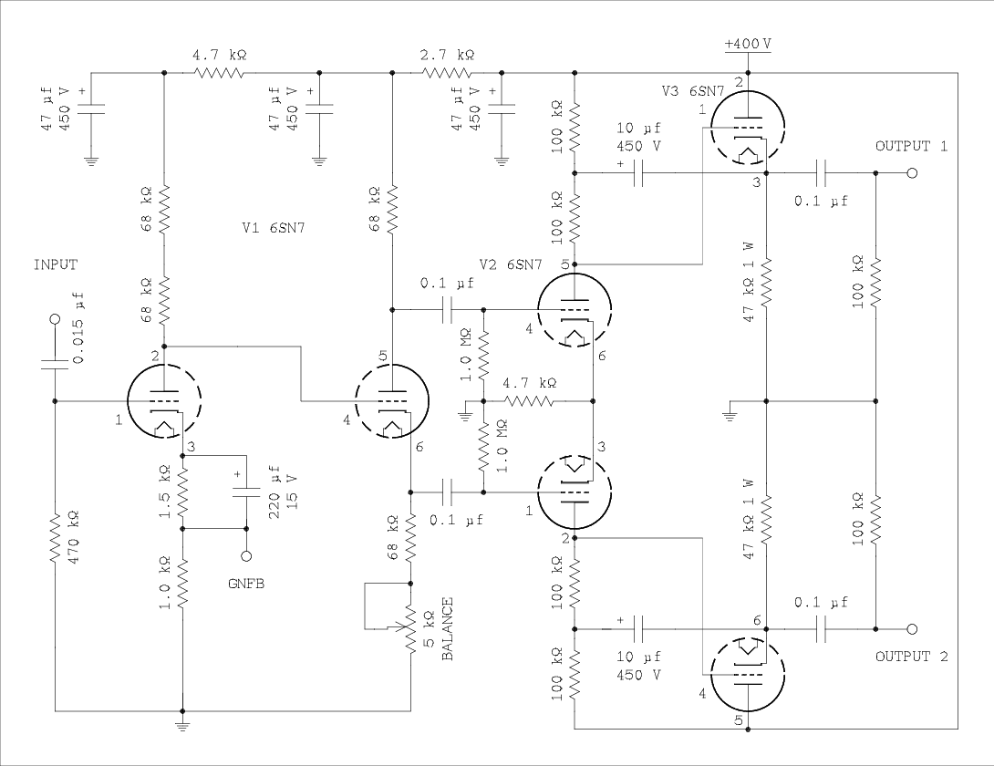
Figure 15 Williamson Circuit With Balance Control and no First Stage Bootstrapping.
For a verbal description click here.
I have left the two 68 k ohm resistors in series in the plate circuit of V1a for a good reason. If a 10 uf 450 V electrolytic capacitor is connected from the junction of the two 68 k ohm resistors to ground the gain is reduced to 170. This almost seems as if it were planned for a required output of 17 volts. If you want to think that I won't get in your way. The distortion at 17 volts output is 0.04/0.075.
The action of the balance control seems counterintuitive. As the balance pot is adjusted the level from output 2, which comes from the cathode of the SLPI, barely changes at all. The level on output 1 is what changes. This makes it easier to adjust than it would be if both outputs changed in opposite directions as the control was rotated.
The reason is the cathode output behaves like a cathode follower. The output voltage is relatively insensitive to changes in the cathode resistor especially when the value of the resistor is large compared to the output resistance of the tube. The gain as measured from the grid to the plate is affected by the value of the cathode resistor so that is where the change is seen.
Changes To John's Design.
I really haven't changed all that much. I removed bootstrapping from V1a because it did nothing to improve the overall performance. I moved the balance control from the plate to the cathode of the SLPI and isolated the pot by putting it in series with the cathode resistor and away from the tube. The pot and its wiring can present some capacitance to ground and effect the high frequency response of the circuit.Final Summary.
I have no doubt that John Wise lived up to his name. Although bootstrapping has been around for decades he decided to apply it to the postinverter amplifier tubes where it is needed most. He saw what engineers have been missing for the last 70 years. Surely his name deserves a place among amplifier designers who have made significant improvements to the audio amplifier art.All in all this is an excellent circuit. Some may find the bottle count a little high but if this is fun with tubes, the more tubes the more fun. As an end to the story here are two oscilloscope screen shots showing the output at 1 kHz and the upper -3 dB point. The pictures speak for themselves.
For a verbal description click here.
THE LONG TAIL PAIR.
The LTP (long tail pair) looks better, from a theoretical standpoint, than an SLPI with no postinverter amplifier. For starters the two outputs are taken from the plates of two triodes. In some earlier testing I did it seemed as though there was a large difference between the amounts of distortion from the two outputs. The differences found here were too small to worry about. Once again I am going to test the phase inverter part of the circuit in isolation. I'll begin with a conventional LTP and later trade the cathode resistor for a current sink. I'm not going to exclude any of the tubes considered above. Many of them have been used in LTP (long tail pair) circuits.
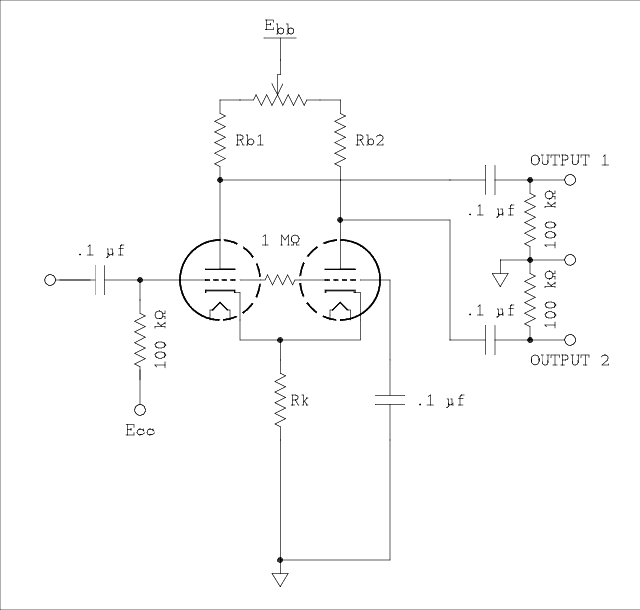
Figure 16 Long Tail Pair With Cathode Resistor.
For a verbal description click here.
| Table 14 Gain and Distortion of a Long Tail Pair With a Resistor in the Cathode. |
|||||||||||
|---|---|---|---|---|---|---|---|---|---|---|---|
| Rb1 = 33 kΩ and Rb2 = 39 kΩ | Rb1 = 47 kΩ and Rb2 = 56 kΩ | ||||||||||
| Tube & Plate | Rk (Ohms) |
Gain | %D @ 17 V |
%D @ 25 V |
f @ -3 dB (kHz) |
Rk (Ohms) |
Gain | %D @ 17 V |
%D @ 25 V |
f @ -3 dB (kHz) |
|
| 6CG7 P 1 | 15 k | 6.88 | 0.121 | 0.211 | 765 | 22 k | 6.94 | 0.144 | 0.27 | 602 | |
| 6CG7 P 2 | 15 k | 6.88 | 0.081 | 0.183 | 795 | 22 k | 5.94 | 0.102 | 0.256 | 622 | |
| 6DJ8 P 1 | 15 k | 11.6 | 0.199 | 0.300 | 923 | 22 k | 11.3 | 0.176 | 0.305 | 713 | |
| 6DJ8 P 2 | 15 k | 11.6 | 0.113 | 0.207 | 1125 | 22 k | 11.3 | 0.122 | 0.263 | 871 | |
| 12AU7 P 1 | 18 k | 6.03 | 0.399 | 0.600 | 730 | 27 k | 5.15 | 0.395 | 0.815 | 539 | |
| 12AU7 P 2 | 18 k | 6.03 | 0.15 | 0.325 | 709 | 27 k | 5.15 | 0.32 | 0.81 | 518 | |
| 12AV7 P 1 | 15 k | 12.3 | 0.204 | 0.36 | 717 | 22 k | 11.7 | 0.215 | 0.355 | 552 | |
| 12AV7 P 2 | 15k | 12.3 | 0.118 | 0.235 | 830 | 22 k | 11.7 | 0.14 | 0.31 | 636 | |
| 12BH7 P 1 | 15 k | 6.64 | 0.32 | 0.495 | 873 | 22 k | 4.64 | 0.365 | 0.545 | 675 | |
| 12BH7 P 2 | 15 k | 6.64 | 0.108 | 0.201 | 803 | 22 k | 4.64 | 0.175 | 0.310 | 615 | |
And the winner is�the 6CG7. The disc jockey tube comes in in second place both in distortion and gain comparison. My favorite horse the 12AV7 came out ahead on gain but distortion is about average for the group. Once again it looks like Tim knew what he was doing.
A couple of notes on procedure are in order. I am using 1% resistors for breadboarding now after finding a kit of them on Amazon. The 39 k ohm plate resistor was trimmed for balance by paralleling larger value resistors with it for equal amplitude as accurately as I can read an analog meter. This was done for each tube and also for the 56 k ohm resistor. For every tube I set Ecc for an Ek value of 125 volts. This should help with direct coupled amplifier stages as previous work reported on this page shows that amplifier tubes prefer higher plate voltages over lower ones. Distortion was fairly insensitive to Ek except when the voltage got up to the neighborhood of 150 to 170 at which point the distortion would rise rapidly.
I think we can completely discount the higher value resistors. None of the tubes showed an improvement with more resistance in their plates.
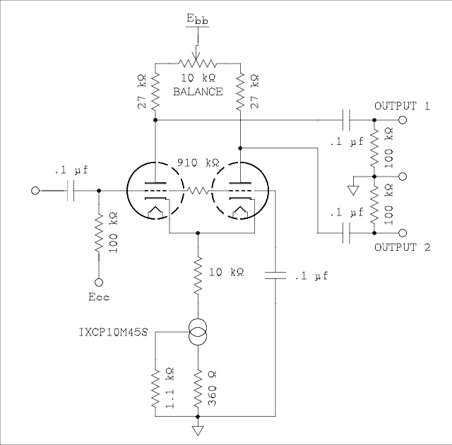
Figure 17 Long Tail Pair as Implemented by Tim.
For a verbal description click here.
The current sink is really a MOSFET that has been selected by the manufacturer for a specific value of transconductance and linearity. In the figure below I have redrawn the current sink as what it really is. I have also changed some of the values originally used by Tim. Changing the source resistor to 330 ohms lowered the distortion at least with the tube I currently have in the socket. Changing the 10 k ohm to a 6.8 k ohm decreased the dissipation of the resistor which was close to 1 watt but it increased the dissipation in the MOSFET. The FET was running quite hot until I installed a small heatsink. One thing I noticed was that as the FET heated up the amount of distortion went down slightly. I don't recommend this as a way to get less distortion.
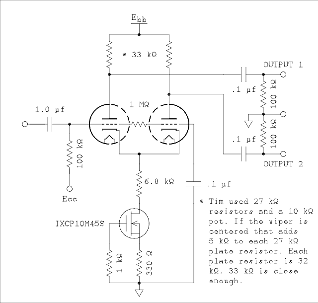
Figure 18 Figure 17 Redrawn Showing Some Value Changes and Current Sink as a MOSFET.
For a verbal description click here.
Now let's see what the same data for the same tubes looks like. Once again I will remind you that I am using 1% resistors.
| Table 15 Gain and Distortion of a Long Tail Pair With a Current Sink in the Cathodes. |
||||
|---|---|---|---|---|
| Rb1 = Rb2 = 33 kΩ Current sink in cathodes. |
||||
| Tube & Plate | Gain | %D @ 17 V |
%D @ 25 V |
f @ -3 dB (kHz) |
| 6CG7 P 1 | 7.69 | 0.0599 | 0.130 | 780 |
| 6CG7 P 2 | 7.69 | 0.0595 | 0.130 | 870 |
| 6DJ8 P 1 | 11.7 | 0.132 | 0.198 | 940 |
| 6DJ8 P 2 | 11.7 | 0.131 | 0.210 | 1130 |
| 12AU7 P 1 | 6.54 | 0.201 | 0.292 | 756 |
| 12AU7 P 2 | 6.54 | 0.235 | 0.359 | 756 |
| 12AV7 P 1 | 12.3 | 0.135 | 0.231 | 730 |
| 12AV7 P 2 | 12.3 | 0.145 | 0.261 | 860 |
| 12BH7 P 1 | 6.56 | 0.202 | 0.32 | 866 |
| 12BH7 P 2 | 6.56 | 0.220 | 0.35 | 866 |
In the category of highest gain�and the winner is�12AV7.
In the category of balanced distortion�and the winner is�6CG7.
In the category of lowest distortion�and the winner is�6CG7.
In the category of widest bandwidth�and the winner is�6DJ8.
For most closely matched upper frequency limits�there is a tie�12AU7 and 12BH7.
Best overall�and the winner is�6CG7.
The miss congeniality award goes to 12AU7.
But What About Intermodulation Distortion.
(Note: Because the IM test signal is made up of two frequencies it has a higher peak value than a single frequency sine wave that reads the same value on a voltmeter. To avoid overdriving the amplifier under test an IM signal must be 80% of the value of a sine wave for a test on the same amplifier.) All values were retested for this table. In the table the capitol letter T stands for tube and the capitol P stands for plate. For example the notation T3 P2 means plate 2 of the third tube. And in case you missed it there is notation in the diagrams above referring to output 1 and output 2. Output 1 comes from plate 1. Pop quiz. Which plate does output 2 come from?
| Table 16 THD and IMD of Long Tail Pair With Current Sink for Different 6CG7s. |
|||||||
|---|---|---|---|---|---|---|---|
| Rb1 = Rb2 = 33 kΩ Current sink in cathodes. | |||||||
| Tube & Plate | THD @ 17 V |
IMD @ 13.6 V |
IMD/THD | THD @ 25 V |
IMD @ 20 V |
IMD/THD | f2 (kHz) |
| 6CG7 T1 P1 |
0.0555 | 0.195 | 3.51 | 0.113 | 0.40 | 3.54 | 858 |
| 6CG7 T1 P2 |
0.0535 | 0.185 | 3.46 | 0.109 | 0.390 | 3.58 | 858 |
| 6CG7 T2 P1 |
0.081 | 0.29 | 3.58 | 0.120 | 0.46 | 3.83 | 815 |
| 6CG7 T2 P2 |
0.0805 | 0.316 | 3.92 | 0.135 | 0.505 | 3.74 | 815 |
| 6CG7 T3 P1 |
0.0435 | 0.145 | 3.33 | 0.0780 | 0.27 | 3.46 | 840 |
| 6CG7 T3 P2 |
0.0430 | 0.190 | 4.42 | 0.0830 | 0.316 | 3.81 | 840 |
| 6CG7 T4 P1 |
0.108 | 0.420 | 3.89 | 0.181 | 0.675 | 3.73 | 880 |
| 6CG7 T4 P2 |
0.105 | 0.420 | 4.00 | 0.182 | 0.675 | 3.71 | 850 |
The IMD/THD ratios are getting a little on the high side compared to the bootstrapped stage which I have already collected the data for although you haven't read it yet. I need to see if I can find a way to improve the linearity at high output levels.
Now I realize I should have made measurements of the long tail pair with only a resistor in the cathode. I set up the circuit again and this time at 17 volts output I got 0.082 and 0.086 for plates 1 and 2 respectively. It's nice to know that the current source improves the distortion figures. Even though I forgot to measure the IMD.
So are we splitting hairs instead of loads? Maybe but the big advantage of the current sink is perfect balance. When I set up the 6CG7 with a 15 k ohm resistor in the cathodes the starting values for the two plate loads were 33 k ohm and 39 k ohm. There was a bit of an imbalance and I corrected it by paralleling a 1.5 meg ohm with the 39 k ohm. This was determined experimentally. With the current sink the two resistors are of equal values and no tuning was necessary. It may seem to be a small improvement of distortion but distortion is like money. A little bit here and a little bit there adds up.
There is something I want to try. All 6CG7s I have seen are packaged in the tall envelope. But some have plates that could be accommodated in a shorter envelope. Tubes 1 and 4 have the tall plates but only 4 has the shield between plates. Looking over the table I don't see any correlation. Testing for the upper -3dB points I get what is shown in the last column of the table which I just added. There is no correlation there either. All measurements were done with the oscilloscope using X10 probes and 3.0 volts input.
What Have We Learned?
Our worst enemy is stray capacitance, as if we didn't already know that. We often need to be reminded of old ideas that we have heard so often that we may easily overlook them. Any imbalance in capacitance in the plate circuits of the two triodes will result in imbalance at the high frequencies leading to distortion in the output of the amplifier. This calls for symmetry of component layout from the phase inverter to the output tubes. Too much capacitance in the cathode circuit will also result in imbalanced drive at the high end. Plate two will have lower output than plate 1. When I connected my DMM to the cathodes the Values of f2 for the two plates were separated by approximately 200 kHz. The measured capacitance of the DMM with leads was approximately 64 pf depending on the relative position of the test leads.Turret board construction is not recommended as it usually involves some rather long leads and symmetry would be well nigh impossible to maintain.
Low Frequency Roll Off of triode 2 Grid Bypass.
One more thing I wish to examine. How does the RC roll off in the grid of triode 2 effect the low end output at each plate. I have argued myself into several different conclusions. I will have to get the correct answer from the breadboard.I changed the one input and two output coupling capacitors to 2.2 μf to get that corner frequency well out of the way. Then used a 1.2 MΩ and a 680 pf silver mica in the grid circuit. The theoretical corner frequency for these values is 195 Hz.
The breadboard should say that the level at both outputs is down by 3 dB at the corner frequency of the resistor and capacitor. The two signals remain 180 degrees out of phase and equal in amplitude as far down as I checked which is 1 Hz. The frequency where the output was down by 3dB was 180 Hz which is a little off from the calculated value. Coming down from 5 kHz I found that the output was down by 0.1 dB at 900 Hz and 1 dB at 350 Hz. This makes the LTP count as one low frequency roll off. Because of the effect of grid current on the operating point of the tube I don't recommend going any higher than 1 MΩ for the grid resistor. A 1 μf cap will bring the corner frequency down to 0.159 Hz. This may be necessary if you are having trouble with low frequency instability or an infrasonic peak.
THE TIM SMITH AMPLIFIER CIRCUIT.
The Preinverter Amplifier.
Even though the LTP has some gain the amplifier that precedes it is no less important. From now on I will assume use of the winning tube which has a gain of 7.69, let's call it 7.7. I will repeat the table from much earlier so I can add to it.
Table 17
Required Gain of Preinverter Amplifier.Tube Type Power Output (W) Drive, Each Tube. (VRMS) Amplifier Gain for
1 V in and 20 dB GNFB6V6GT 14 10.6 13.8 6L6/G/GT 26.5 15.9 20.6 6L6GC 55 24.7 32.1 EL34 54 25 32.5 EL34 UL 34 25 32.5 6550 EBB=400V 55 17 22.1 6550 EBB=600V 100 23 29.9 Now that's more like it. All gains are easily obtainable without going to extremes.
Tim's amplifier stage.
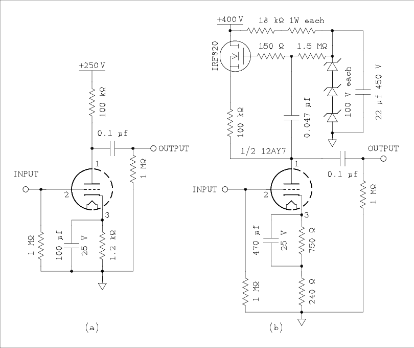
Figure 19 a Standard Resistance Coupled Amplifier Stage
b Amplifier with Bootstrapped Load Resistor in the Plate Circuit.
For a verbal description click here.
Tim used a 12AY7 with bootstrapping as the amplifier stage before the long tail pair analyzed above, figure 17b. The MOSFET is a source follower which makes the upper end of the load resistor track the lower end. Tim informed me that he had used components he had on hand. I was forced into the same situation which accounts for the different values I used in the circuit. For example two 18 k ohm 1 W resistors to take the place of a 36 k ohm 3 watt.
How It Works.
The gate of the MOSFET is at the same DC potential as the cathode of the top zener diode, 300 volts. The gate of a MOSFET as the closest thing in electronics to an open circuit. With no direct current flowing through the series combination of the 1.5 meg ohm and 150 ohm resistors there is no voltage drop across them. This is an enhancement mode device so the source is a bit more negative than the gate but it is only a few volts. To all intents and purposes the source is at a DC potential of 300 volts.So the 100 k ohm resistor connects between a 300 volt DC source and the plate of the tube. The 0.047 μf capacitor couples AC signal from the plate of the tube to the gate of the MOSFET. For this test the only load on the plate circuit of the tube is the 1.5 meg ohm resistor. The other end is at AC ground potential. The MOSFET source follower does what source followers do, the source follows the gate. A duplicate of the AC plate voltage is applied to the top end of the 100 k ohm load with only a slight attenuation. (Note: If the gain were exactly unity the circuit would be unstable and tend to ring. Just a skinch more than unity and it would oscillate.)
The AC signal at the plate which is transferred to the upper end of the 100 k ohm resistor through the FET causes the upper end to move up and down in potential, (AC), in step with the lower end. This means that while there is a direct current through the resistor there is almost no alternating current. For AC the effective resistance at the plate is very high, limited by the 1.5 meg ohm resistor which is capacitively coupled to the plate. The result is that the gain is very nearly equal to the amplification factor (μ) of the tube. The 12AY7 has a μ value of 40 and as you can see in the table below the values of gain fell very close to that, except for number 7 which is an outlier for every measurement made on it.
Repeated below is a table which I included earlier. It has much more relevants now. The plate voltage and gain fall right into the wheel house of the long tail pair. I have also included IMD and high end corner frequency. For the most recent version of the LTP the drive required to produce 25 volts output is 3.25 volts. THD will be remeasured at this level of output from the 12AY7 along with the IMD. Testing a simple RC amplifier will give us a base line against which to judge the improvements resulting from the increased complexity. After filling in this table we will install the bootstrapping in the plate to see how it changes the performance of the stage. Then more columns will be added to the table to reflect the results. As you read these words you are seeing the complete table. Conclusions will be drawn below.
Table 18
Data on Several 12AY7sEbb = 250 VDC, Vout = 3.25 VAC
Rb = 100 kΩ, Rk = 1.2 kΩ
Figure 17aEbb = 400 VDC, Vout = 3.25 VAC
Rb bootstrapped, Rk = 750 Ω + 240 Ω
Figure 17bTube Eb Gain %THD %IMD f2 (kHz) Eb Gain %THD %IMD f2 (kHz) RC Data 109 29 0.6 12AY7 1 114 31.5 0.263 1.19 290 127 39.4 0.142 0.27 120 12AY7 2 112 31.8 0.269 1.1 276 126 40.2 0.135 0.25 110 12AY7 3 110 30.3 0.27 1.13 294 125 38.1 0.136 0.292 120 12AY7 4 110 29.9 0.188 0.80 257 125 38.4 0.129 0.152 100 12AY7 5 112 30.1 0.211 0.95 271 126 38.4 0.130 0.182 110 12AY7 6 120 31.2 0.295 1.26 267 135 40.2 0.140 0.284 100 12AY7 7 103 25.2 0.599 2.83 329 116 31.2 0.645 0.94 140 Now it becomes apparent what it is about Tim's amplifier that makes it sound so good. Look at the ratios of IMD to THD for figure 19a. For tube 4 the value is 4.25. The rest fall into that neighborhood. Now look over to the data for the bootstrapped amplifier, figure 19b. Tube 4 comes in with a ratio of 1.18. All tubes fall generally between this value and 2 with one outlier, tube 3, at 2.15.
In the construction article for the IM analyzer I went into great detail with plenty of mathematics showing the difference between the effect of THD and IMD on the listener. In a nutshell it amounts to this. Harmonic distortion if not too severe is in tune with the music but IM distortion is decidedly out of tune. That makes it much more unpleasant as it falls on the ear. Bootstrapping the amplifier and a current sink in the LTP reduce both kinds of distortion but they decrease the out of tune kind much more than they do the in tune kind. Bootstrapping the plates of the LTP would without a doubt reduce the amount of IM distortion even further.
SPOILER ALERT! When the amplifier and long tail pair phase inverter were connected together the distortion was so low that nothing further is necessary. What little improvement there might be wouldn't be worth it.Figure 19b has two low frequency roll offs. One is the 0.047 μf and 1.5 meg ohm in the bootstrapping circuit. The other is the bypassed cathode resistor. I can't convince myself that when the plate is bootstrapped, bypassing or not bypassing the cathode resistor has any effect. The math says no effect as follows. The gain for an amplifier with an unbypassed cathode resistor is given by,
AV = -μ Rb / (rP + Rb + Rk[μ + 1]) Rb is the load and because it is bootstrapped it is very high, perhaps approaching infinity. So we find the limit as Rb approaches infinity of the equation above. The first step is to divide numerator and denominator by Rb. The result is,
AV = -μ / (rP/Rb + 1 + Rk/Rb[μ + 1]) Now that Rb appears in the denominator as it approaches infinity the terms rP/Rb and Rk/Rb will approach zero. That leaves us with,
AV = -μ /1 This calculation is for a circuit like figure 17b except that the capacitor across the cathode resistor is missing. I did find that if both resistors in the cathode are bypassed by a single capacitor the upper corner frequency is increased by about 50%. This is caused by a lowering of the output impedance which happens when the cathode resistor is bypassed.
Removing the 470 μf capacitor shown in figure 8 will reduce the gain by about 1 dB. The equation above says "no change" but Rb, the 100 k ohm resistor, does not approach infinity. In the test circuit There are 4 resistors that make up the load.
- The bootstrapped 100 k ohm.
- The 1.5 meg ohm resistor that provides DC bias to the gate of the MOSFET.
- The 1 meg ohm resistor to ground after the 0.1 μf DC blocking capacitor.
- The 1 meg ohm input resistance of the HP 334A distortion analyzer.
(Note: Obviously in a real circuit the distortion analyzer will not be connected. That takes away one of the 1 meg resistors. The 0.1 uf cap and 1 meg ohm resistor will still be there. They are just connected in the other order.) If I knew what the gain of the MOSFET was I could calculate the effective resistance of the bootstrapped resistor. I can only guess what the gain is. My attempts to measure it resulted in a burned out FET, 3 shorted zeners, and an exploded resistor in the Fluke power supply. If you can explain how these three things relate causally, you're a better man than I am.
I entered the gain equations for a triode first with Rb = infinity then with 100 k ohms. Then with a bypassed and unbypassed cathode resistor into a spreadsheet.*
What this calculation showed was that when the load is changed from the high value of the paralleled 1 meg, 1 meg, and 1.5 meg, resistors to the 100 k ohm in parallel with these the gain is reduced by 2.66 dB. Removing the 0.047 μf capacitor removes the bootstrapping from Rb and reduces its resistance to 100 k ohms. This reduces the measured gain by 2.6 dB.
The math also told me that when the bootstrapping in the plate is working and the cathode bypass capacitor is removed the gain is reduced by 0.8 dB. Removing the capacitor from the breadboard reduced the measured gain by 1 dB. That's really pretty good considering all of the errors that can creep into tube circuits.
* I have found that a spreadsheet is a faster means of programming equations than any dialect of BASIC.
Evaluating the effect of the low frequency roll off caused by the 0.047 μf cap and 1.5 MΩ resistor was accomplished by substituting a much smaller capacitor for the 0.047 μf. The roll off didn't seem to be right so I simply removed the capacitor. The gain was reduced by 2.6 dB. The point is that as the coupling capacitor to the MOSFET gate rolls off the gain, it can only drop by a maximum of 2.6 dB and then goes flat again. This is the low end analog of connecting a series RC in parallel with the signal path to achieve the same effect at the high end. The value of the bootstrapping capacitor could probably be used to frequency compensate the low frequency end.
Note. It is not my intention to publically embarrass Tim. He doesn't have test equipment to make measurements in the infrasonic range so he didn't know about the low end response of his amplifier. When his second amplifier came into my hands there was an infrasonic peak around 2 to 3 Hz. I can't be any more definite because the peak was at a different frequency depending on whether I came at it from above or below. This hysteresis effect indicated instability. I cured it by reducing the values of the coupling capacitors between the LTP and the output tubes. Now that I have a better understanding of the circuitry maybe I can take a more scientific approach to taming those infrasonics.The burned out MOSFET had an interesting fallout. When I replaced it the THD came in at 0.058%. I had thought that the 22 uf capacitor in parallel with the string of zener diodes was redundant so I left it off. The MOSFET only survived one on/off cycle of the B+. The fluke circuitry is arranged so when the switch is changed from standby to on, the voltage comes up almost instantaneously. When the switch is changed from on to standby the output becomes an open circuit. If there is no B+ filtering capacitor on the breadboard the voltage will fall as quickly as it came up upon turn on. What must have happened was that the drain and source voltages fell to zero so quickly that the relatively slow discharge of the 0.047 uf capacitor pulled the gate outside its limits burning out the MOSFET. The 22 uf capacitor was restored and the third FET gave a distortion figure of 0.069% with IMD of 0.17%. You are probably thinking "Oh no, not another table." I think the point has been made. Select your fets.
I have been informed of two MOSFETs that will perform better in this circuit than the IRF820. They are the IRFBC20 and ZVN0545A. The IRFBC20 has a lower reverse capacitance and the ZVN0545A has an even lower one. The former is in a TO220 package while the latter is in a TO92 package. It may not stand up to the power dissipation requirements of this circuit. Perhaps one of them will increase the upper end roll off. There's no knowing what it will do to the distortion. I have some of each on order. Stay tuned.
Substituting the IRFBC20 had no effect on either distortion or upper frequency roll off.
I needed to investigate how the amplifier would deal with GNFB (global negative feedback). For this I set up the circuit variation shown in figure 20.
Figure 20 Test Of Injecting Signal at the Cathode.
For a verbal description click here.
What I found was that when signal is fed to the amplifier stage through the cathode connection rather than the grid its behavior was essentially the same as when signal is fed to the grid. There is nothing to worry about here.
Connecting them together.
I have both the 12AY7 amplifier stage and the 6CG7 LTP on the breadboard. All I need to do is run a wire between them.
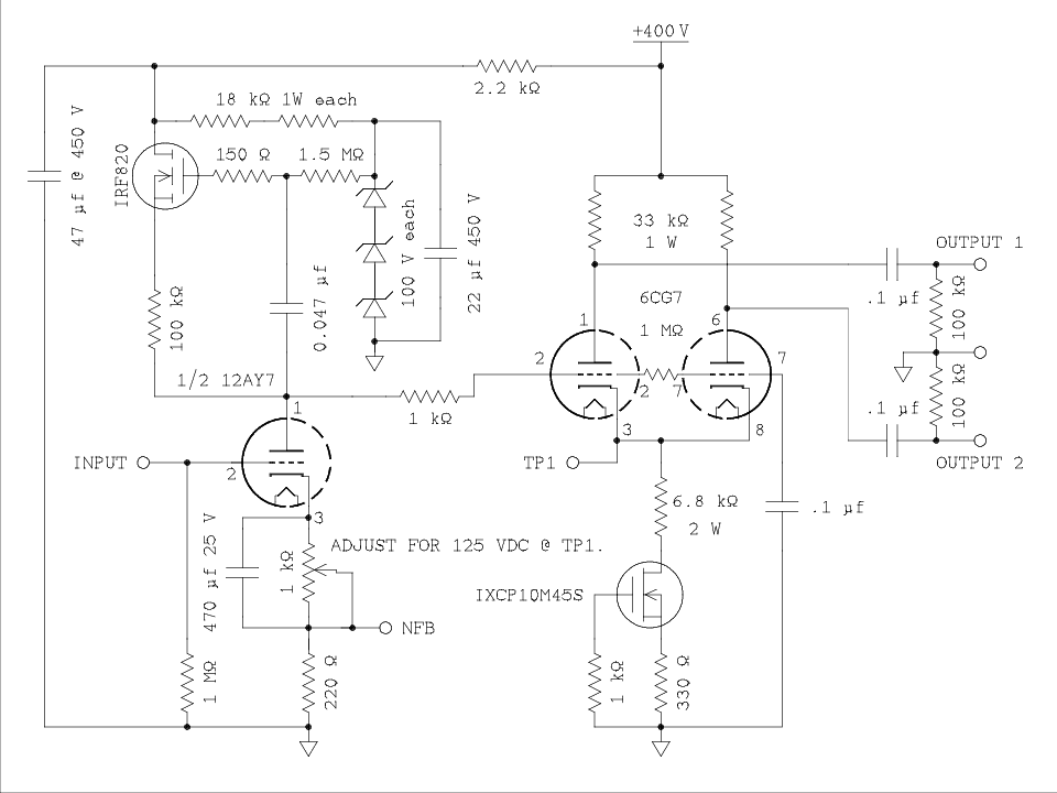
Figure 21 Schematic of Complete Amplifier & Long Tail Pair.
For a verbal description click here.
Here is the data for the bootstrapped amplifier and long tail pair with current sink.
Plate 1 @ 17 V, THD = 0.088%, @ 25 V, THD = 0.090%
Plate 2 @ 17 V, THD = 0.094%, @ 25 V, THD = 0.098%
Plate 1 @ 13.6 V, IMD = 0.21%, @ 20 V IMD = 0.265%.
Plate 2 @ 13.6 V. IMD = 0.22%, @ 20 V IMD = 0.290%.
Frequency response: -3 dB @ 58.3 kHz, -6 dB @ 102 kHz,-10 dB @ 175 kHz, and -20 dB @ 578 kHz.
These readings are for plate 1. At the highest frequency plate 2 was about 5% below plate 1.After seeing the f2 numbers from the John Wise circuit I wish they were better for this circuit. The problem is the bootstrapped amplifier ahead of the LTP. Because the LTP has gain it has a significant Miller capacitance. I'm sure the FET has a gain closer to unity than a tube which means that the amplifier using it will have a higher output impedance than one that is not bootstrapped. The 1 k ohm grid stopping resistor is too small to produce the measured roll off for any reasonable amount of Miller capacitance.
As I write this I have just finished with the John Wise circuit. I did the Tim Smith LTP circuit first. It seems as though I have been working on this project for years. More realistically months. I just looked it up and the earliest file date on a figure is January 27, 2018. Today is June 14, 2018. So I'm not far from having been working on this article for 5 months. At the present time I'm not inclined to go back and work on it some more. Maybe when I get around to building an amplifier using some of what I have learned I'll feel more like trying to add a little more knowledge to the phase inverter book.I can hardly believe those distortion numbers myself. I performed the measurements several times. I could have wished for someone who could check my work but Sue is not electronically literate. I made the measurements and made them again. Then I walked away from the workbench, got a drink of water and came back to do it again. There were small variations in the third decimal place but no serious errors turned up. After returning from the drink I did the measurements again and they came out the same. I left power on while I was away so everything was well warmed up. Then I measured the IMD. I have placed the results above for easy comparison to the THD data. I want to assure you that the drink I took really was water. The distortion figures are so small that some may call my competence into question. It's bad enough being nearly blind. Being drunk too would be the last straw.
Changing the enhancement mode MOSFET that is in the plate circuit of the 12AY7 has almost no effect on performance. Changing the depletion mode MOSFET that is in the cathode circuit of the 6CG7 has very little effect on performance. Trying 4 different 6CG7s while keeping the same 12AY7 produced a THD high of 0.177 at 25 volts output. Keeping the same 6CG7 and trying 6 different 12AY7s resulted in some readings as low as 0.079 but none were above 0.1. I adjusted the pot for each tube. Looks like we have a winner.
Conclusion.
Whether or not he graduated from Georgia Tech, I can say with certainty that Timothy E. Smith is one hell of an engineer.Without a doubt the Tim Smith circuit is a very good one. Maybe I am waxing overly enthusiastic but I think the Tim Smith amplifier deserves to go into the Parthenon of amplifiers alongside the Williamson and ultra linear circuits. Although I have one that was built by Tim himself I still have the urge to build one of my own. It's just a matter of time. If I can find a means of reducing the distortion of the output tubes it might even be possible to build an amplifier with no GNFB.
Someone has already pointed out to me that the distortion inherent in output tubes is much higher than that measured in these phase inverter circuits. I am sure I measured distortion in a pair of 6550s that were being driven by a very low distortion inverter circuit that was well below 0.5%. Unfortunately I didn't document the measurement so I need to go back and measure it again. I guess my next project will be to examine various output tubes to see if there is anything that can be done to reduce their distortion. Meanwhile, have fun.
This page last updated Monday, July 22, 2019.