
Photo of Newcomb D-10.
Photo of Newcomb D-10.
The little Newcomb D-10 has been around for a long time and it just won't seem to go away. It came out of the factory with an inadequate amount of negative feedback and as a result had more distortion than I would have wished for. On the page where I first demonstrated the use of Bode plots I thought it would be a good example. It turned out to be a good example of failure. Even though this amplifier is never used in an entertainment system for me it is an unsolved problem. I hate unsolved problems. To me they are a contest not won. I can't let this thing beat me.
I was literally in the middle of preparing that article when the SysComp CGR101 came in. I started using it right away, maybe before I had completely learned how. They had come out with the 201 some time ago and I finally decided it was time to update.
As I looked back over the other article I realized that I had omitted one step. This seems like a perfect excuse to return to the Newcomb and present the complete procedure.
Where to start.
If you have not spent a lot of time with Bode plots I strongly urge you to follow the link above and study, not just read, the material down to the heading "Example 2, the Newcomb D10."If you are working on a newly completed amplifier it won't have any compensating capacitors installed. But this reclamation project had them and they needed to be removed. That included one little capacitor that I must now admit I missed seeing on the schematic. It's a 47 pf capacitor from the plate of the amplifier section of the 12AX7 to ground. I found the physical capacitor when I was replacing the coupling capacitors which were long overdue. This capacitor flattened out a little peak at the high end but it probably got in the way when I was trying to apply lag compensation to that same point. It has been removed. First the schematic.

Figure 1 Schematic of Newcomb D-10 with all compensating capacitors removed.
Step 1, Finding the Output Impedance of the Plate Circuit of the 12AX7 Amplifier Stage.
Before we connect up our instrument and begin making plots there are some rules that need to be followed.We can't calculate much of anything without knowing the output impedance of the first triode amplifier in figure 1. At audio frequencies it is safe to assume that the impedance is resistive so I really meant output resistance.
- Proper grounding.
Improper grounding can result in data that is totally meaningless because of unintentional positive or negative feedback introduced through ground loops. Connect only one ground from the CGR101 and connect it to the point where the secondary of the output transformer goes to ground. This amplifier used the chassis as common ground so I clipped the CGR101 ground to the point where the secondary connected to the chassis, namely a solder lug on the rectifier tube socket. If you clip the ground lead to the 8 ohm dummy load the resistance of the wire between the amplifier and the load will apply some of the output signal back to the input which is unwanted feedback. I recommend grounding the channel B input cable. Also there is no need to use X10 probes. The circuits here are low impedance.- Grounding the grid of the first stage.
The connection used causes the cathode of the first stage to be driven by the signal generator. The amount of capacitance between cathode and grid is sufficient to couple signal from cathode to grid within the test band of frequencies. The cathode is the inverting input and the grid is the noninverting input. If both are driven in phase there will be very little output. Because this amplifier uses contact bias I couldn't just short the grid to ground. I used a 0.1 μF capacitor with alligator clips attached to its leads.I have experimented with several ways of measuring the output resistance and most of them agree with one another. Given the equipment available the capacitor roll off method seems to be the easiest. A known capacitor is connected from the plate to AC ground which in this case is B+3. In other words the capacitor is connected in parallel with the 270 k ohm resistor. The specific capacitor is a 0.0018 uf 5% 500 volt capacitor. Xc = R at the frequency where the phase is lagging the mid band phase by 45 degrees.

Figure 2Finding Output Resistance of 12AX7 Amplifier.
The mid band phase is 180 degrees so the 45 degree lag value is 135 degrees. The cross cursor doesn't show up on the print screen function but the coordinates that are attached to it do. They are 1.419 kHz, 135.6 degrees. So,
Xc = 1 / (2πfC)
Xc = 1 / (6.283 x 1419 x 0.0018 x 10-6)
Xc = 62.3 k ohms.
Ro = 62.3 k ohms.
Step 2, Finding the value of Rf.
For the above plot the value of Rf was still an unknown so I used a 1 k ohm. Spoiler alert, that wasn't very far off. The first thing that must be done is to measure the open loop gain, A, by injecting a signal at the wiper of the pot and measuring the output voltage at the 16 ohm tap on the output transformer. Turn the volume control pot to at least half rotation. I did this measurement with a meter rather than the CGR101 (Circuit Gear) scope to obtain the best accuracy. The value was 88.1.The loop gain is measured by passing the signal through the feedback factor network which has the value B and then through the amplifier which has a gain of A. These two values are expressed as ratios of output to input, (whether gain or attenuation). When the two are cascaded, that is the output of one is connected to the input of the other, The values multiply to give the overall gain. Hence, the loop gain is given as
AL = AB
If the value of AL is known we can calculate the value of B as follows. The value of A has been measured as 88.1.
9 = 88.1 B
B = 9 / 88.1 = 0.102
Now we use B to find the value of Rf
B = Rk / (Rk + Rf)
Solving for Rf gives,
Rf = Rk(1 - B) / B Rf = 100 (1 - 0.102) / 0.102 = 880 ohms.
Of the two standard values on either side of 880, 820 is 60 ohms away while 910 is 30 ohms away. So 910 it is.
Step 3, Deciding How Much Lag To Apply.
Now you see two copies of the loop gain, A B, plotted over a limited frequency range. The cursor was used to read out the frequencies of the two breakpoints, BP1 and BP2, at phase shifts of 135 and 45 degrees respectively.

Figure 3a CGR101 Analyzer Plot of Newcomb D-10 Showing 1st Break Point With All Compensating Capacitors Removed.

Figure 3b CGR101 Analyzer Plot of Newcomb D-10 Showing 2nd Break Point With All Compensating Capacitors Removed.
The problem with the above plots is that when the phase gets very close to zero the gain is still approximately 10 or 11 dB. If we were to close the loop the amplifier would oscillate at a frequency slightly higher than 100 kHz. Remember that the method of connecting our test instruments gives 180 degrees as negative feedback and zero degrees as positive feedback. We need to find a way to lower the gain at 100 khz by at least 11 dB. Although we may be getting ahead of ourselves we don't try to stabilize an amplifier with lag alone. We do as much with lag as is practical then achieve final stability by using lead compensation.
A Lag Network, What It is, What It Does, and How It Works.
Real lag networks are made of 2 real resistors and one real capacitor -- or are they? In audio amplifiers the output resistance Ro of an amplifier stage takes the place of one of the resistors. This resistor can't be seen or touched but electrically it is as real as any other resistor. This means that the value of one of the resistors is forced upon us and we must calculate the values of the capacitor and the other resistor to go with it.

Figure 4a Schematic Of An Example Lag network.
In figure 4a above, Ro is the output resistance of an amplifier stage. Its presents in the diagram tells us that C1 and R1 are connected in series in the plate circuit of an amplification stage somewhere in the amplifier. Sometimes they are connected from the plate to ground and sometimes they are connected in parallel with the plate load resistor. This is the design engineer's choice and it makes little or no difference.
At low frequencies the gain of the amplifier is the same as it would be if C1 and R1 were not there. When the frequency is reached where the reactance of C1 is equal to the sum of Ro and R1 the gain of the amplifier will be down by 3 dB from the low frequency value and the phase shift will lag the low frequency phase angle by 45 degrees. This is the first breakpoint. As the frequency continues to increase the amplitude continues to decrease falling at the rate of 20 dB per decade. The phase will trend toward 90 degrees. Whether it actually gets to 90 will depend on how widely the two frequencies are separated from one another.
When the frequency reaches the point where the reactance of C1 equals the value of R1. The actual frequency response curve begins to level off. At this frequency the amplitude is down by
3 dB + 20 log ( R1 / (R1 + Ro) ) dB
from the low frequency value. The phase has returned to 45 degrees lagging from the low frequency value. The reason for adding 3 dB to the gain is that the gain curve is coming down from above and at the second breakpoint it is 3 dB above the gain value that it will eventually settle on. This is the second breakpoint.
The Bode plot is not a smooth curve but is the tangents to the curve. At the first breakpoint the plot breaks from a horizontal line to a downward sloping line. At the second breakpoint the line breaks suddenly from sloping back to horizontal as shown in figure 4b below.

Figure 4b Bode Plot Of An Example Lag network.
On the Bode plot the frequency and amplitude at the first breakpoint are,
f1[/Hz] = 1 / (2πC1(Ro + R1)),
A1 = Alf
respectively. Where f1 is the frequency of the first breakpoint, Ro, C1, and R1, are as shown in figure 4a, A1 is the gain at breakpoint 1, and Alf is the low frequency gain of the amplifier stage. At breakpoint 2 the frequency and gain are,
f2[/Hz] = 1 / (2πC1R1),
A2 = Alf R1 / (R1 + Ro) = Alf f1 / f2,
respectively. f2 is the frequency of the second breakpoint and A2 is the gain at the second breakpoint.
Determining Component Values In Figure 4a.
Ro is set by tube parameters and to a somewhat lesser degree by resistor values in the amplifier stage. Its value was determined from figure 2 and the calculations which followed. The value was found to be 62.3 k ohms.R1 comes from the equation above for A2.
Alf R1 / (R1 + Ro) = Alf f1 / f2
We now solve this equation for R1. Alf will cancel and we divide through by (R1 + Ro and f2 to obtain,
R1 f2 = f1 (R1 + Ro),
Expanding the term on the right,
R1 f2 = f1 R1 + f1 Ro,
Collecting R1 terms,
R1 f2 - R1 f1 = Ro f1,
Factoring out R1 and dividing gives,
R1 = Ro f1 / (f2 - f1) ohms.
C1 = 1 / (2πf2R1) farads.
Ro = 62.3 k ohms.
Determining the frequency span.
There isn't really a formula for deciding on the breakpoints, f1 and f2, for a lag network. It comes down to engineering judgment. We have the benefit of a failed attempt done on this same amplifier several years ago and described on the page where I first demonstrated the use of Bode plots. Look at example 2.I was seriously handicapped by that capacitor from the plate of the 12AX7 to ground. Without it I now have a first breakpoint of 33.1 khz instead of 9.5 as before. The second breakpoint has also moved up a little which can help.
In that earlier failed attempt I used a 1 octave frequency span for the lag network. The second breakpoint of the lag network is always equal to the first breakpoint of the amplifier. That placed the two breakpoints at 4.75 and 9.5 khz respectively. Now with an amplifier first breakpoint of 33 khz we can use a larger span and really push the bad behavior down below unity gain. I decided to set the first breakpoint of the lag network to 5 khz. With that decision made we can calculate the values of R1 and C1.
Given,
f1 = 5 khz.
f2 = 33 khz.
Ro = 62.3 k ohms.
Calculated.R1 = Ro f1 / (f2 - f1) = 62.3k 5k / (33k - 5k) = 11.1 k ohms.
C1 = 1 / (2πf2R1) = 1 / (2 x 3.1416 x 33k x 11.1k) = 434 pf
R1 is really close to 11 k ohms and if 5% capacitors came in 5% steps as resistors do I would have a 430 pf cap. But they don't so I don't. So should I go up to 470 pf or down to 390 pf? Using a 390 pf will move both breakpoints up in frequency by 10% which will not push the misbehaving parts of the phase graph down in amplitude as far. On the other hand using a 470 pf cap will move both breakpoints of the lag network down in frequency which will push the bad phase farther down in amplitude. Sounds like a 470 pf is preferred.
Recalculating f1 and f2.
f1 = 1 / (2πC1(Ro + R1)) = 1 / (2 x 3.1416 x 470e-12 x (62.3k x 11k)) = 4.62 khz.
f2 = 1 / (2πC1R1) = 1 / (2 x 3.1416 x 470e-12 x 11k) = 30.8 khz.
Now we put these values on the Bode plot.
Step 4, Applying The Calculated Lag Network To The Amplifier.

Figure 5 Bode Plot Of Real Lag Network Applied To Real Amplifier.
The blue line is the lag network, The red line the original amplifier, and the green line the sum of the blue and red lines which makes it the response of the amplifier with the lag network installed. I put dots anywhere the lines break to a different slope. Note the two dots that are slightly overlapping on the green line. The line goes horizontal for a short distance. I no longer need to wonder if I made the right choice by going up in capacitance. Now I can see it. If I had gone down in capacitance the blue line would have been shifted to the right and the slope of the green line would have gone to -2 for a short distance. Either way the curve isn't going to show much of an effect. It would be just a little bump in both gain and phase curves that would hardly be noticeable.
What we are doing is giving up some upper frequency response to obtain stability. Giving up upper frequencies is not desirable but when it is made necessary by an inferior output transformer, well, what else can be done. In an ideal universe we would junk the existing output transformer and replace it with one of higher quality. In this case for reasons of sentimentality and nostalgia nothing that is visible from the top of the amplifier can be changed.
In figure 5 the lag network response breaks down to a slope of -1 where the response of the amplifier itself is still flat. Where the amplifier response breaks down to a slope of -1 the network response breaks back to being flat. Thus the composite response breaks to a slope of -1 at the first breakpoint of the network and continues on that same slope until the amplifier's second breakpoint. At least that's how it works with ideal slopes and breakpoints. As will be done below the lag network values need to be fudged a little to bring the behavior closer to the ideal.
Now what's the next step? Although in the other article I went directly to applying the lead capacitor I actually skipped a step.
Step 5, Soldering The Real Components Into The Amplifier And Graphing It.

Figure 6 Plot of D-10 With Lag Network Installed Showing phase margin.
The lag network that was installed for the graph in figure 6 above consisted of a 470 pf capacitor and an 11 k ohm resistor. The Bode plot shows breakpoint 2 at 70.8 khz while the graph of the amplifier shows it to be 48.5 khz. But more disturbing is the small phase margin. The gain crosses zero dB at 67.920 khz. As shown in figure 6 the phase margin at this frequency is 6 degrees. With the second breakpoint being so close to the unity gain frequency the lead compensation won't add very much to the gain and phase margins. We need to do as much as we can with the lag network. What this means is some cut and try.
I will spare you each step of the trial and error process. I wound up with a 470 pf capacitor and a 4.7 k ohm resistor. There's nothing magic about these numbers. That's just how things worked out.

Figure 7 Plot of D-10 With Trial And Error Lag Network Installed Showing phase margin.
The phase margin is now 26.4 degrees. That would not be good by itself but the lead network doesn't need to do as much work as it would have for a 6 degree phase margin.
Step 6, The Lead Network.
The second breakpoint is at 63.9 khz. The lead capacitor now becomes,C = 1 / (2πf2Rf) = 1 / (2π63.9k x 910) = 2.7 nf = 0.0027 μF.
The lead network starts its work at the frequency where the amplifier's response breaks from a -1 slope to a -2 slope. At this same frequency the lead network's Bode plot breaks from 0 to a slope of +1. As shown in figure 8 below when combined with the amplifier's Bode plot the +1 slope turns the -2 slope into a -1 slope thus improving the phase margin.

Figure 8 Theoretical Bode Plot Showing Effect Of Lead Network.
Because the real amplifier isn't very well behaved at ultrasonic frequencies the lead circuit doesn't accomplish nearly as much as the theoretical one.

Figure 9 Real Lead Network Applied To Real Amplifier.
The black line is the plot with no capacitor connected across the feedback resistor Rf. The red line is for a 0.0027 μF capacitor.
Again there was some trial and error to be done to improve gain and phase margin. Not much could be done but changing Cf to 0.0033 μF helped some. And that's about as far as I can go. Making the capacitor any larger only made things worse.
Step 7, Closing The Loop.
With the loop closed up I made the following measurements.

Figure 10 Plot of D-10 With Loop Closed Up Showing Overall Frequency Response.
Information Read From This Graph While It Was Live On the Screen.
Center Frequency Gain = 18.53 dB.
10 kHz Gain = 17.73 dB, -0.80 dB down from mid band.
20 kHz gain = 16.29 dB, -2.24 dB down from mid band.
Zero dB gain at 112.2 kHz.The phase crosses 180 degrees at 81.3 kHz where the gain is 10.4 dB. Intuition says the amplifier should oscillate at this frequency yet the square wave test shown below gives only the slightest hint of ringing. Converting dB to gain gives 3.20. The value of B by
B = Rk / (Rk + Rf) = 100 / (100 + 910 = 100 / 1010 = 0.0990.
The loop gain which is AB is 3.20 x 0.0990 = 0.317. Converting back to dB gives -9.98 dB which is the gain margin. This is better than I had hoped for and the reason why the square wave response, although not perfect, is as good as it is.
The first and second breakpoints as found by locating the 45 and 135 degree phase shifts are 17.88 kHz and 66.6 kHz respectively.

Figure 11a 1 kHz Square Wave Response Showing Approximately 2 Cycles of the Wave.

Figure 11b 1 kHz Square Wave Response With Rising Portion Stretched Out For Easier Examination.
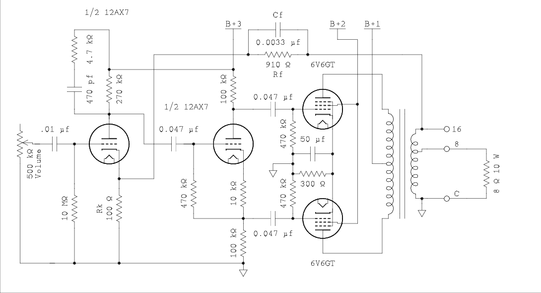
Figure 12 Schematic Diagram Of Completed Modifications.
Final Measurements.
Open loop gain to 16 ohm tap = 88.1
Open loop gain to 8 ohm tap = 61.5Open loop THD = 0.460% at 1/2 watt output into 8 ohms.*
Loop gain = 9.62
Closed loop gain = 8.58 on 16 ohm output tap.
Closed loop gain =5.90 on 8 ohm output tap.Closed loop THD = 0.059% at 1/2 watt output into 8 ohms.*
* 8 ohm load connected to 8 ohm tap.