On April first 2019 I received an email message from Circuit Specialists notifying me that they had added a semiconductor curve tracer to their product line. For many years, decades now, I have owned a Heathkit semiconductor curve tracer adapter that plugged into a standard oscilloscope. Its maximum voltage is 200 volts which is marginal for vacuum tubes. Somehow it never worked very well on tubes.
The one from C S has a maximum test voltage of 500 volts which is not only enough to give you a good shock it is plenty for amplifier triodes as well as low and medium power pentodes. And it works with BJTs and FETs to boot. And it was on sale.
To get to the page click here. The link still works but the price has gone up. I did say I got it on sale.
Although I do occasionally work with discrete transistors and integrated circuits I tinker around with vacuum tubes more often. Therefor my primary reason for buying the new curve tracer is to use it with tubes. To that end I designed and built a tube test fixture to plug into the tracer. But first I will begin with a product review. Following that you will find an exhaustive if not exhausting operating tutorial.
Review.
The tracer is shown in the photo at the top of this page. It is exactly what it looks like, a traditional oscilloscope with the sloping test panel at the bottom of the front as first done by Tektronix in their original vacuum tube curve tracer and since used in their semiconductor curve tracer and copied by HP and others including this latest example. As you can tell the curve tracer is based on an old fashioned, some may say obsolete, CRT oscilloscope. I will refrain from speculating on why this decision was made but given a choice I would prefer a DSO (digital storage oscilloscope) style.The CRT (Cathode Ray Tube.
I don't wish to dwell on this but the tracer did need some warranty work. Circuit Specialists made good on it so I am happy. If you scroll down the page to the heading "Calculating Power Dissipation in the DUT" and look at the next three screen shots just below it you will see the screen of the first tracer I had. When it was returned after being repaired it was not the same unit. You can see in most of the other screen shots on this page photos of the one I currently havethat the graticule is etched on a transparent material which is in front of and outside the CRT. In some of the pictures you will see the one with the internal graticule and others with an external one. If you decide to buy one of these tracers I cannot say which kind you will get. I don't think the CRT was replaced. There didn't seem to be any reason for doing that.The CRT has a considerable amount of astigmatism. Enough to send you reaching for the astigmatism control if it had one. When I open up the scope I hope to find an internal control. If I am really lucky it will be placed so I can drill a hole in a side panel for screwdriver access to it.
There is no scale illumination on the CRT so if pictures of the display are taken in total darkness the grid lines become invisible. An illuminated scale would make it possible to lower the intensity of the CRT which would give a sharper display. The camera could be mounted in a shroud which would not only provide total darkness regardless of room lighting but would always hold the camera in the same position.
The only alternative I can come up with is to tripod mount the camera and take pictures under normal room lighting. The scanning is slow enough that a 1/10 second exposure time is necessary. That's too slow for a hand held shot. In regions of the world which use 50 Hz electricity the exposure may need to be even longer. Eventually I'll take the covers off the scope to see if scale illumination can be retrofit.
The Oscilloscope Section.
On the X (horizontal) axis it will display voltage between base and emitter, or gate and source, from 0.05 to 2 volts / div set in the familiar 1, 2, 5, sequence. By continuing to rotate the same control it will display voltage between collector and emitter, or drain and source, from 0.05 to 50 volts / div. There is an additional section labeled VR and printed in red. This goes from 100 to 500 volts / div. These highly dangerous voltages have not been enabled on this unit. I think this is a wise decision. Reverse or forward voltage can still be applied to a diode and measured using the VCE settings.On the Y (vertical) axis it will display reverse diode current from 0.2 to 10 micro amps. Continued rotation of the control will allow display of collector or drain current from 0.02 milli amps to 1 amp.
The other standard oscilloscope controls you would expect to find are there. Positioning controls, an inverting switch that works simultaneously on both axes, and brightness, focus, and trace rotation, for the CRT. And not to be forgotten, power on/off and a power on indicator LED.
Power Supplies For The DUT (Device Under Test).
Collector Supply.
For the collector supply there are a series of pushbuttons that select the peak voltage to be applied to the collector or drain of the DUT. They are 5, 20, 100, and 500 volts. Each voltage has a different maximum current. They are, respectively, 10A, 2.5A, 0.5A, and 0.1A. There is an analog control that permits setting the peak voltage anywhere from zero to the voltage selected by the pushbuttons. It is calibrated 0 to 100%. Part of the collector supply is a switch that selects values of resistance from 0 to 500 kOmega; set in a 10, 50,. 250, sequence. The lowest nonzero value is 0.5 Ω. This control is labeled with the name "SERIES RESISTANCE Ω". More about this name in the next section. Its purpose is to limit the current available to the DUT to avoid burning it out. This is no guarantee that you will never burn out a transistor you are attempting to trace. The operation section of this page will present a number of rules that will help prevent burnouts. Even that is no guarantee. The most important control is the one between the ears of the operator.In curve tracers from Tektronix and HP/Agilent/Kassite the collector voltage sweep is linear upward and the beam is blanked for the return trace. In lower cost tracers, such as this one, the voltage sweep is derived from the AC line and is half of a sine wave, going up and coming back down with a rounded top. This system has its advantages and its disadvantages. The main advantage appears to be low cost. Among the disadvantages are, a sweep rate which is low enough to cause visible flicker on a large family of curves, extra circuitry which is required to compensate for phase shifts and time delays that cause up and down traces to not fall on top of each other, and an increase in trace brightness near the end of each curve as the rate slows down at the peak of the sine wave.
The failure of up and down traces to line up needs more explanation. An example will illustrate. Suppose that a BJT (bipolar junction transistor) is being traced with a peak collector voltage of 20 volts. On its way up to 20 volts it passes through 10 volts. Suppose at this point going up that the current is 1.25 mA. Now on its way back down the voltage once again passes through 10 volts but this time the current is 1.21 mA. This is hysteresis. Meaning that the current depends on whether the voltage came up from below or down from above. The value depends on its history. Economizing on the generation of collector voltage requires some additional circuitry and two controls. I wonder if this is a false economy.
Hysteresis is caused by phase shifts and time delays in the circuitry. The two controls labeled LOOPING and COMPENSATION are provided to permit the hysteresis effect to be canceled out. When adjusting these controls a false optimum point can be found. It may look good but if you add more steps by adjusting the number of steps control every other trace will look really bad. If you want to take a picture for publication be sure to adjust these controls with the number of steps set to the desired number for the illustration.
STEP GENERATOR.
The controls in this part of the panel adjust the circuitry that generates a stare case or stare step function. So called because of its appearance when viewed on a second oscilloscope. The function is a current for BJTs and a voltage for FETs. The main control sets the value of each step change. For BJTs the range is from 1 micro amp per step to 100 milli amp per step. For FETs the voltage is from 0.5 V/step to 2 V/step. The name of this control is "STEP/OFFSET AMPL". I wouldn't have called it that. I would have left out the "/OFFSET" and completely spelled out, amplitude calling it STEP AMPLITUDE. But the designers didn't consult me.The number of steps control is an analog control that behaves like a digital one. This seems to be common practice among curve tracer designers. Even the Heathkit tracer used this way of setting the number of steps.
The "OFFSET" control may lead to confusion because of the use of that same word on the step amplitude control. In this case the offset is what one might expect by the name. It adds a variable voltage or current to the stare step function. The added quantity is zero at mid rotation and goes negative or positive depending on the direction of rotation off center. Pushbutton controls on the test set help in adjusting the offset control. Their function in conjunction with the control will be described under the "TEST SET" heading.
Another potential source of confusion for the user is the "SERIES RESISTANCE Ω" set of pushbuttons. This is exactly the same name given to the rotary switch in the collector/drain supply. A trade school teacher or university professor who is writing up a lab experiment employing the curve tracer must be very careful to specify which "SERIES RESISTANCE Ω" he or she means.
Supplied Test Fixtures.
A total of 5 test fixtures were supplied with this instrument. Two will accommodate TO92, TO5 or TO220 transistors.

Two will hold TO3 transistors,


and the remaining one has clips to hold the leads of diodes.

Overall Evaluation.
With all of the above said the performance is not bad. It does not come up to that of a Tektronix or HP, But what do you expect for 766 dollars. It outperforms the Heathkit model IT-1121 going away even when the latter is plugged into a modern high quality DSO. I give it 4 stars out of 5 and would recommend it to anyone who can say they are competent to operate a curve tracer.Dimensions: measured as it sits on my bench. H x W x D 13-5/16" x 9-9/16" x 21-1/2". Including Chrome plated knobs on front. When the power cord is plugged into back it protrudes about 2 inches beyond the depth dimension.
Weight: 29.76 pounds. If you are over 75 be sure your medical insurance is paid up before lifting it up to your workbench.
Price: $765.92
Available From Circuit Specialists.
CSI4810A Instruction Manual.
In this section of this page I have endeavored to remove anything that seems to be too much like review material and give just the facts mam. If I have failed in places it may be because I felt that such comments would help to enlighten the user. My aim with this entire page is to help someone decide if they want to buy this instrument as well as learn how to operate it safely and effectively.The Curve Tracer in General.
Every curve tracer can be divided into two main subsystems. 1) An X-Y oscilloscope, and 2) A set of voltage and current sources that can be swept or stepped to run the device under test (DUT) through its operating range. The latter can be further subdivided into two parts, 2a) the bias supply for the base of a BJT or the gate of an FET, and 2b) the collector or drain supply. The base/gate supply is usually stepped while the collector/drain supply is usually swept. Recently, some DIYers have suggested that when the scope is a DSO (digital storage oscilloscope), that random noise or even music can be used as the collector/drain supply.If you think an oscilloscope is hard to operate, you've never tried to run a curve tracer. It has most of the complication of an o'scope plus the controls for applying the proper voltages and currents to the device under test (often abbreviated DUT). A curve tracer is not a suitable instrument for the service shop. However, for the serious electronics experimenter it can be a real time saver.
When a graph of characteristic curves of a tube or transistor is presented in a data sheet or book it is referred to as a family of curves. This term will appear throughout the following description of the curve tracer. This device draws the family of curves on its screen. From this graph you can derive the current gain or transconductance of the DUT as well as output resistance, plate, collector, or drain.
A curve tracer plots voltage on the horizontal axis and current on the vertical one. At first glance some of the controls will be familiar but others may be a complete mystery. There is no time / div setting. It presents an XY display.
The oscilloscope Section.
On the vertical scale the current is displayed in micro amps, milli amps, and even amps. The horizontal scale shows the voltage that is applied to the DUT. An advanced tracer may also have the capability to select the voltage that is being plotted such as collector to emitter or base to emitter.There are positioning controls for both X and Y axes. There is also a switch in common to X and Y axes for reversing the display so the curves of a PNP BJT or P channel FET will not appear upside down.
Those who are well acquainted with the operation of an oscilloscope should not have any difficulty figuring out this part of the curve tracer control panel.
Device Test Conditions Settings.
Any good curve tracer has controls for setting,
- the maximum collector or drain voltage of the DUT,
- the base current of a BJT,
- the gate voltage of an FET,
- The reverse current of a diode for leakage testing.
Collector/drain voltage sweep.
The collector/drain voltage sweep is set by a set of controls that select the maximum voltage to be applied to the DUT as well as limit the current. In some tracers the voltage sweep is derived from the AC line and is half of a sine wave, going up and coming back down with a rounded top. In others the voltage is a linear sweep going up. The return trip is prevented from writing to the screen.This voltage control most often takes the form of A switch that sets a number of maximum voltages each with its own current limit. The higher the voltage the lower will be the maximum current. In conjunction with this switch is an analog control for setting the percent of the switch setting. The calibration on this control is from zero to 100%. The first thing to do is to set the horizontal and vertical sensitivity to the least sensitive ranges. The maximum voltage controls should be set and then the volts/div of the scope section set so the trace does not go off the screen. A third control in this grouping is the limiting resistance. The resistance should be set much greater than V/I where V and I are the values of voltage and current set on the Maximum voltage switch. Additional information will be provided in the section on tracing specific kinds and case styles of transistors.
Current to Base or Voltage to Gate.
The other setting for the DUT is the base current of a BJT or the gate voltage of an FET. Selecting the proper value for the setting of the control is quite involved and will be covered in greater detail in the "Curve Tracer Operation" section below. Provisions are made for reversing the gate voltage to allow tracing of depletion or enhancement mode MOSFETs.The first step in setting the base current is to set the vertical scale, current / division to a range that will cause the display to go off scale as the current through the DUT approaches damaging values. Then the base current is set to the lowest possible range. Then the DUT is plugged in and the base current advanced until the display covers a large part of the screen.
FETs are different. When the gate voltage is set to the lowest range the drain current will be at maximum. The vertical scale can be set to show the current. The family of curves will be very close together. As the gate voltage range is advanced the family will spread out and be distributed over the entire screen.
An Operating Tutorial. This Instrument in Particular.
As well as a detailed review, see above, this article will also include thorough operating instructions. The operating manual that comes with this instrument is written in clear English although the syntax is a little unusual in places. The problem with it is it is rather brief. The writer appears to have assumed that the reader is already familiar with curve tracers in general. Many details of operation have been omitted.Curve Tracer Description.
It is exactly what it looks like, a traditional CRT oscilloscope with the sloping test panel at the bottom of the front as first done by Tektronix in their original tube curve tracer and since used in their semiconductor curve tracer and copied by HP and others including this latest example.The Controls, Oscilloscope Section.
HORIZONTAL VOLTS/DIV.

The VOLTS/DIV knob has 3 distinct areas. Starting at the fully clockwise position they are VBE base to emitter voltage on a BJT or gate to source voltage on an FET, VCE collector to emitter voltage on a BJT or drain to source voltage on an FET, and VR reverse voltage on a diode. The highest voltages, up to 5000 volts have not been implemented on this tracer. When the switch is rotated from 50 volts/div to 100 volts/div the voltage goes to zero. However the reverse characteristics of a diode can still be explored up to 500 volts.
There is a funny symbol at the fully counter clockwise end of the VOLTS/DIV and CURRENT/DIV controls. If the +/- locking pushbutton in the STEP GENERATOR area is in the + position (out) and the volts and current controls are set to the symbol a trail of dots goes diagonally up the screen. This is for calibration. The tiny dots are useful for adjusting the FOCUS control. These settings are supposed to be for adjusting horizontal and vertical positioning while a device is being traced. Because the baseline of the traces shifts slightly as the voltage / div or current / div controls are rotated, these adjustments can be made with greater accuracy just by looking at the displayed family of curves and adjusting for the bottom line on the bottom grid line and the dot at the lower left corner of the family to the left grid line. These adjustments are critical if transistor parameters are to be read from the curves.
The TRACE SEPARATION control works only when the DUAL button on the TEST SET is pushed in. It will be explained when the topic of matching transistors is discussed.
The position control works the same as on any oscilloscope.
VERTICAL CURRENT/DIV.

The CURRENT/DIV knob has 3 distinct areas. Starting at the fully clockwise position they are IR reverse current of a diode in microamps that is connected to the IR test jacks, IC collector current of a BJT or drain current of an FET in mA milliamps. And finally is IC in amps for some real power. The x0.5 pushbutton will double the size of the display in the vertical dimension.
The position knob works exactly the same as on any other oscilloscope you have ever used.
The INV (invert) locking pushbutton inverts both vertical and horizontal when pushed in. This is to permit viewing of the curves of PNP transistors or P channel FETs without standing on your head.
Biasing the DUT (device under test).
COLLECTOR SUPPLY. Collector / Drain Supply Voltage.
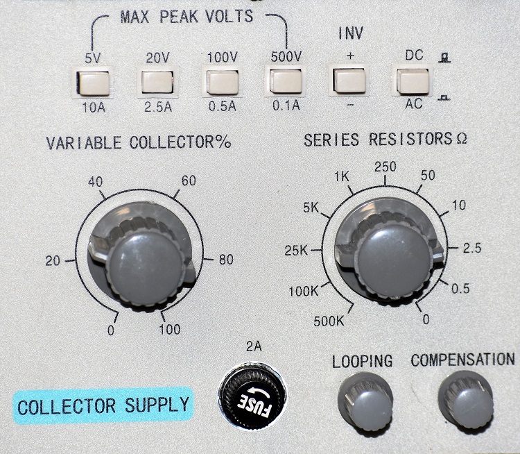
The MAX PEAK VOLTS is a set of radio buttons. They select voltages of 5, 20, 100, and 500 volts at maximum current ratings of 10, 2.5, 0.5, and 0.1 amps respectively. The "INV" button permits changing the polarity of the voltage to negative for PNP BJTs or P Channel FETs. The DC / AC button permits applying the full cycle of the line to the DUT. This may be useful for testing triacs or some kinds of diodes. The VARIABLE COLLECTOR% knob is an analog control which permits adjustment from 0 to 100% of the selected value of peak voltage.
The SERIES RESISTANCE Ω selects a wide range of values. These are set to prevent the DUT from dissipating too much power. But this is no guarantee that you won't burn out a transistor while trying to trace it. You will find many precautions in the operating instructions section.
FUSE, LOOPING, and COMPENSATION Controls.
At the bottom of this area of the panel you will find a fuse and two knobs. The fuse is marked 2 amps. It seems unlikely that it is in the secondary side of the collector supply circuit since the 5 volt pushbutton gives a power supply current of 20 A. It is probably on the primary side of a transformer. The manual is silent on this matter.The collector supply is derived from the power line and so is a half cycle of the line frequency. This means that the voltage and current go up and come back down. The main problem with the up and down approach is loops caused by phase shift and delay. The two controls are used to adjust out the loops. You may think that one setting fits all but this is not so. If you set the vertical range switch to .02 mA/DIV you will get what appears to be a high sensitivity indicator of proper adjustment for the LOOP and COMPENSATION controls. But when you start playing with the NUMBER OF STEPS control you will see that every other number of curves gives a good set of curves while the alternate numbers give a very bad one. You must adjust the two controls for the best looking family of curves for all settings of the NUMBER OF STEPS control. Adjust them in an alternating sequence to obtain the best looking display.
STEP GENERATOR. Base Current or Gate Voltage.

The STEP/OFFSET AMPL knob sets the amount by which the current or voltage changes with each step. It has three distinct areas. They are milliamps for power BJTs, microamps for small signal BJTs, and volts for FETs.
Below the OFFSET knob is a locking pushbutton that is marked only with the symbols + and - (plus and minus). This is the polarity reversing control.
- Use plus for NPN BJTs, P-channel depletion mode FETs, and N-channel enhancement mode FETs.
- Use minus for PNP BJTs, N-channel depletion mode fets, P-channel enhancement mode FETs, and vacuum tubes.
Below the step control is a set of radio buttons that, unfortunately, have exactly the same name as those in the COLLECTOR SUPPLY area of the panel. These buttons select the value of resistance that is in series with the base/gate supply. I'm not certain of the reason for this added series resistance. When operating as a source of base current it is a current source. And as we all know a perfect current source has infinite impedance. Add any number to infinity and you've still got infinity. When the step generator is supplying gate voltage to an FET the source resistance should be as low as possible to be sure of fast switching of the stair step function. This is especially true for high capacitance MOSFETs. Some resistance could be permitted to protect the voltage source against shorted devices. Since we have some choice set the resistance to the middle value of 10 k ohms. If the display doesn't look right you can always change it to 1 k ohm.
To the right of the three resistance selector buttons are two more that allow a change from continuous display to single sweep. When the button labeled REP / SNG is pushed in, the display is turned off. When the second from the right is pressed the family of curves is swept once.
This feature was probably included to permit photography that is free of uneven brightness from some lines being scanned once and others scanned twice while the shutter was open. The procedure would be to set the camera shutter on BULB, hold the shutter open, and press the SGL / PUSH button, then close the shutter. This requires a camera mounted in a shroud for complete darkness. But the problem is there is no scale illumination on this scope. The scale lines are only visible where they are crossed by a trace line and it is impossible to make accurate readings from a picture.
The only solution I can come up with is to tripod mount the camera and take pictures under normal room lighting. The scanning is slow enough that a 1/10 second exposure time is necessary. That's too slow for a hand held shot. In regions of the world which use 50 Hz electricity the exposure may need to be even longer.
The NUMBER OF STEPS is an analog control that acts like a digital one. When the knob is fully counter clockwise five levels are generated which gives rise to 5 curves in the family. As the knob is rotated clockwise curves are added one by one until the total number reaches eleven.
The OFFSET control is a bit tricky to adjust. When tracing a BJT the OPEN button on the TEST SET panel is depressed and held, while the position of the single line is noted. It is usually desirable to adjust the vertical position control to place the line exactly on the bottom line of the grid scale. Then the OPEN button is released and the OFFSET is adjusted so the very bottom line of the family of curves falls on the bottom line of the grid. When tracing a depletion mode fet or a vacuum tube the SHORT button is depressed and held. All but the uppermost curve will disappear. Release the short button and adjust the OFFSET control until the top curve of the family is in the same place it was when the SHORT button was depressed. This adjustment can be made easier by repeatedly pressing and releasing the SHORT button.
POWER AND CRT Controls.

The OFF ON locking pushbutton turns the unit off when out, and on when in.
The red POWER LED indicates that power is on.
The INTENSITY control adjusts the brightness of the display.
The FOCUS control adjust the focus of the display.
The TRACE ROTATION permits a screwdriver to be used to align the CRT trace with the grid lines on the screen.
There is no externally accessible astigmatism control. Too bad. It neads one.
TEST SET.

The TEST SET is where the transistor test fixtures are plugged into sets of banana jacks to connect the DUT to the testing circuitry. There are pushbutton controls to set the mode of operation and help with adjustment of the controls on the oscilloscope front panel.
LEFT, RIGHT, and DUAL, radio buttons.
When the LEFT button is pressed the testing circuits are connected to the left hand set of jacks. When the RIGHT button is pressed the testing circuits are connected to the right hand set of jacks. It is suggested that you begin the test of a transistor by pressing the button opposite to where you want to plug in the transistor or test fixture containing the transistor. Then plug in the transistor and press the button for the side where you plugged in the device. Also you should end the test by pressing the button opposite to the side where the device is plugged in and then remove it from the fixture or unplug it from the tracer. This is the best way to avoid self inflicted shocks.When the DUAL button is pressed switching circuitry in the test set alternates connection between left and right jacks. When DUAL mode is used the locking pushbutton above the DUAL button must be correctly set for BJT (TRANS) or FET devices.
The two remaining buttons are to aid in adjusting the OFFSET control in the STEP GENERATOR area. They are both spring return buttons. The OPEN button is used in conjunction with BJTs. When it is held down the base connection is opened setting the base current to zero. The OFFSET control is adjusted so the bottom line of the family of curves does not change as the button is depressed and released.
The SHORT button is used in conjunction with depletion mode FETs and vacuum tubes. When it is pressed the gate is shorted to the source, (grid shorted to cathode). When the button is pressed and held all but the top most curve disappear. The OFFSET control is adjusted so that the one remaining curve aligns with the top most curve of the family.
Tracing a BJT.
Calling a three terminal semiconductor device a transistor is incomplete information. "Do you mean a bipolar junction transistor or a field effect transistor?" You could call it a non FET but it seems more economical of ink to call it by the initials of its name, BJT. Apparently the Chinese engineers who designed this puppy weren't well enough acquainted with the English names of things to know this. With that little detail out of the way we can get on with it.A curve tracer is not a simple device to operate. I used to have my students at the university do a lab experiment around the Heathkit unit. (My department head was not willing to buy one that was more sophisticated than that.) The result was two or three burned out transistors a year and a blown fuse in the tracer every couple of years. The reason is there is not one right setup for a given transistor. It depends on what it is about the device the user wants to see.
Rules of Thumb To Avoid Burning Out a Transistor Under Test.
It is assumed that you will not memorize this entire section. This is intended as a reference document which you will access and look up the particular transistor style you are tracing at the moment. For this reason there is redundant information in each section. For example the phrase " Setup the Tracer Before Connecting the Transistor." Will appear in the section for each style. If you just read through everything you will be saying "Why the hell didn't he just say it once and get it over with?" But where do I say it so everyone who uses this page as a lookup reference guide will see and read it? In each style section.Settings for Polarity and Type, BJT/FET.
Determine the polarity of the transistor you are going to test. Here are the proper settings.NPN BJT.
INV button on blue line between VERTICAL and HORIZ sections: Out, +
INV button in COLLECTOR SUPPLY area: Out, +
+/- button in STEP GENERATOR area: Out, +
PNP BJT.
INV button on blue line between VERTICAL and HORIZ sections: In, -
INV button in COLLECTOR SUPPLY area: In, -
+/- button in STEP GENERATOR area: In, -
N Channel FET.
INV button on blue line between VERTICAL and HORIZ sections: Out, +
INV button in COLLECTOR SUPPLY area: Out, +
+/- button in STEP GENERATOR area: In, -
P Channel FET.
INV button on blue line between VERTICAL and HORIZ sections: In, -
INV button in COLLECTOR SUPPLY area: In, -
+/- button in STEP GENERATOR area: Out, +
Settings for Different Case Styles.
BJTs Only.
To-92, TO-5, and Similar Sizes, without heatsink.
Setup the Tracer Before Connecting the Transistor.
MAX PEAK VOLTAGE: 20 volts.
VARIABLE COLLECTOR %: 90.
SERIES RESISTANCE in the COLLECTOR SUPPLY section: 1 k.
For TO-5 and TO-92 CURRENT/DIV: 1 mA/div.
For TO-220 CURRENT/DIV: 2 mA/div.
VOLTAGE/DIV: 2V/div in the VCE section of the control.
STEP/OFFSET AMPL: 1 μA.
SERIES RESISTANCE in the STEP GENERATOR section: 10 k.
NUMBER OF STEPS: fully counter clockwise.
OFFSET: center of rotation.
Connect the transistor and depress the correct left or right button. Advance the STEP/OFFSET AMPL clockwise until the display is as large as it can be without overflowing the screen.
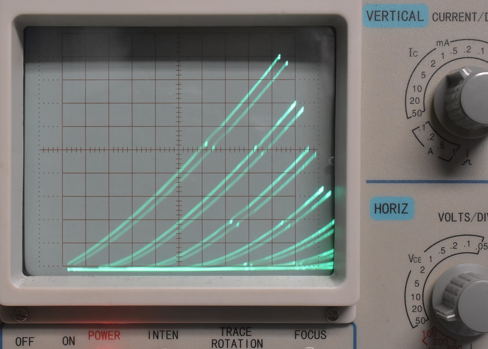
The setting of the STEP/OFFSET AMPL control which gave the display pictured below was 5 μA / step.
If you do not get any deflection the BJT is most likely bad. At these settings the transistor will become warm to the touch.Adjusting the OFFSET CONTROL for a BJT.
When tracing a BJT it is possible to deceive yourself and misadjust the OFFSET control. Be careful! With a normal BJT family of curves on the screen press and hold the OPEN button on the TEST SET. While continuing to hold the button adjust the vertical position control to position the line exactly on the bottom grid line on the screen. Release the OPEN button. Turn the OFFSET control in the STEP GENERATOR area of the control panel. Note that the whole family moves up and down. But no curve moves below the bottom grid line. Turn the offset control fully clockwise to be sure you are seeing the bottom most curve. Turn the control counter clockwise until this trace falls exactly on the bottom grid line. Stop turning at this point. Press and release the OPEN button a few times to be sure the bottom trace does not move.

Family of Curves of a 2N3904.
Determining the β parameter.
While the DC forward current gain often is symbolized by HFE, most experimenters know it as beta (β). So let's say we are going to use the transistor in an amplifier at VCE = 10 V and IC = 2.0 mA. The first curve comes the closest to that but the idiot who took the picture didn't have the zero reference line exactly on a line. It is at -0.15 dib. The first curve passes through 10 volts at 1.8 div therefore the vertical distance between zero and the first curve is 1.8 + 0.15 = 1.95 div. With a vertical setting of 1 mA / div the collector current is 1.95 mA. The base current setting is 5 μA /step so the base current is 5 μA.β = IC / IB = 1.95 mA / 5 μA = 390
That seems somewhat high for a 3904 but it is confirmed by my universal component tester.
Determining hfe.
The use of lower case letters indicates an AC value. The AC values of device parameters are defined without calculus as,hfe = Δic / Δib Where the symbol Δ is read as "change in". It would be nice if we had more curves but this is what we in fact have. The change in collector current between the first and second curves is exactly 2 mA. The change in base current is exactly 5 μA so the AC current gain is 400. If you have equipment for measuring the current gain at a specific frequency you will likely come up with a different value at high frequencies. But that's another instrument for another review.
Voltage Gain of an amplifier, hie and Gm.
The voltage gain can be defined in two ways. The first is,Av = RL hfe / hie
and
Av = RL Gm
Where RL is the parallel combination of all resistances that are both DC and AC coupled to the collector of the transistor. This can include the effective input resistance of the next amplifier stage which could be the hie of the transistor. And Gm is the transconductance of the transistor under examination.
Determining the values of Gm and hie.
What we need to find hie is a plot of base current versus base to emitter voltage. We almost have it. What we have is a plot of collector current versus base to emitter voltage. All we need to do is divide IC by hfe.

Plot of IC versus VBE.
For this trace we have switched the horizontal range switch from the VCE ranges to the VBE ranges. At 0.1 V / div the curve is not spread out very much. Switching to the next more sensitive range 0.05 V / div the pattern goes off the screen. But it can be brought back by adjusting the horizontal position control. We can no longer see the zero point but we don't need to. This is called suppressed zero operation and can be used when only voltage differences are required. What we are setup to measure is the transconductance of the transistor.
Gm = ΔIC / ΔVBE.
Where Gm is the transconductance of the transistor. Some algebraic calisthenics will lead us to,
hie = hfe / Gm.
The proof of this is left to the reader.
The points we are interested in are the first two points on the approximately straight part of the curve. The horizontal difference between these two points is 0.03 div which for a setting of 0.05 V / div is 1.5 mV. The vertical distance looks like 2.1 div which at a setting of 1 mA is 2.1 mA. However we have better information than this curve. Above we already determined that the vertical distance between curves in the family is 2 divisions. We also learned from the family that the value of hfe is 400. Based on this we come up with the following values.
Gm = 2 mA / 1.5 mV = 1.33 mhos.
This could be expressed as 1,330 milli mhos or the way it's done in a vacuum is 1,330,000 micro mhos.
hie = hfe / Gm = 400 / 1.33 = 300 ohms.
Yesterday is dead and gone. And tomorrow's out of sight.
H parameters are definitely from yesterday. As a matter of fact it's been more yesterdays than I care to remember. The three authors of the book "Experimental Methods in RF Design" have shown a simple way to determine the transconductance of a BJT and shown that the gain equations are much simpler using that parameter. We old dogs often have trouble learning new tricks but whether you are an old dog or a young pup, it appears that transconductance is the way to go.Breakdown Voltage.
If you want to increase the voltage to discover the secondary breakdown voltage, decrease the base current setting to minimum and increase the amount of SERIES RESISTANCE Ω to a very large value such as 100 kΩ. DO NOT TOUCH ANY METAL PARTS OF THE TRANSISTOR WHILE MAKING THIS TEST.

Plot showing secondary breakdown. Horizontal voltage range = 10 V / div..

Plot showing VCEO. Open button on Test Set pressed and held..
TO-220, TO-202, and similar sizes, without heatsink.
Setup the Tracer Before Connecting the Transistor.
MAX PEAK VOLTAGE: 20 volts.
VARIABLE COLLECTOR %: 90.
CURRENT/DIV: 10 mA/div.
VOLTAGE/DIV: 2V/div in the VCE section of the control.
STEP/OFFSET AMPL: 1 μA.
NUMBER OF STEPS: fully counter clockwise.
OFFSET: center of rotation.
Connect the transistor and depress the correct left or right button. Advance the STEP/OFFSET AMPL clockwise until the display is as large as it can be without overflowing the screen. If you do not get any deflection the BJT is most likely bad.At this setting the transistor will become warm to the touch. If you want to increase the voltage to discover the secondary breakdown voltage, decrease the base current setting and increase the amount of SERIES RESISTANCE Ω to a very large value such as 100 kΩ.
Adjusting the OFFSET CONTROL for a BJT.
When tracing a BJT it is possible to deceive yourself and misadjust the OFFSET control. Be careful! With a normal BJT family of curves on the screen press and hold the OPEN button on the TEST SET. While continuing to hold the button adjust the vertical position control to position the line exactly on the bottom grid line on the screen. Release the OPEN button. Turn the OFFSET control in the STEP GENERATOR area of the control panel. Note that the whole family moves up and down. But no curve moves below the bottom grid line. Turn the offset control fully clockwise to be sure you are seeing the bottom most curve. Turn the control counter clockwise until this trace falls exactly on the bottom grid line. Stop turning at this point. Press and release the OPEN button a few times to be sure the bottom trace does not move.TO-3, and similar sizes, without heatsink.
Setup the Tracer Before Connecting the Transistor.
MAX PEAK VOLTAGE: 20 volts.
VARIABLE COLLECTOR %: 90.
CURRENT/DIV: 20 mA/div.
VOLTAGE/DIV: 2 V/div in the VCE section of the control.
STEP/OFFSET AMPL: 1 μA.
NUMBER OF STEPS: fully counter clockwise.
OFFSET: center of rotation.
Connect the transistor and depress the correct left or right button. Advance the STEP/OFFSET AMPL clockwise until the display is as large as it can be without overflowing the screen. If you do not get any deflection the BJT is most likely bad.At this setting the transistor will become warm to the touch. If you want to increase the voltage to discover the secondary breakdown voltage, decrease the base current setting and increase the amount of SERIES RESISTANCE Ω to a very large value such as 100 kΩ.
Adjusting the OFFSET CONTROL for a BJT.
When tracing a BJT it is possible to deceive yourself and misadjust the OFFSET control. Be careful! With a normal BJT family of curves on the screen press and hold the OPEN button on the TEST SET. While continuing to hold the button adjust the vertical position control to position the line exactly on the bottom grid line on the screen. Release the OPEN button. Turn the OFFSET control in the STEP GENERATOR area of the control panel. Note that the whole family moves up and down. But no curve moves below the bottom grid line. Turn the offset control fully clockwise to be sure you are seeing the bottom most curve. Turn the control counter clockwise until this trace falls exactly on the bottom grid line. Stop turning at this point. Press and release the OPEN button a few times to be sure the bottom trace does not move.Depletion mode FETs Only.
To-92, TO-5, and Similar Sizes, without heatsink.
Setup the Tracer Before Connecting the Transistor.
MAX PEAK VOLTAGE: 20 volts.
VARIABLE COLLECTOR %: 90.
CURRENT/DIV: 2 mA/div.
Feel free to change this setting if the trace goes off the screen or only comes up a little distance from the bottom.
VOLTAGE/DIV: 2V/div in the VCE section of the control.
STEP/OFFSET AMPL: .05 V.
+/- button: Pushed in minus (-).
NUMBER OF STEPS: fully counter clockwise.
OFFSET: center of rotation.
Connect the transistor and depress the correct left or right button.Adjusting the Offset control For an F E T.
Rotate the Offset control in the STEP GENERATOR area of the control panel. Note that the entire family of curves moves up and down as you do so. Press and hold the SHORT button. This places a short between gate and source. Note that a single trace appears. Release the button. Because you just disturbed it the top trace of the family probably is not in the same place as the single trace. Repeatedly press and release the SHORT button while adjusting the OFFSET control until the top trace is in exactly the same place as the single trace that appears when the button is pressed.You should now see something like this.

The STEP GENERATOR always starts from zero regardless of the polarity setting. When the gate to source voltage of a FET is at or very near zero the drain current is at a maximum.* Rotate the STEP/OFFSET AMPL counter clockwise and you will see the traces separating and moving down from the top most one which doesn't move. You can adjust the STEP/OFFSET AMPL and the NUMBER OF STEPS controls to obtain a display that looks the way you want it. Something like this.

* because the gate to channel is a silicon PN junction it is possible for the bias to be up to 0.6 volts positive without any gate current. A junction FET can be operated in this region although it is rarely done in practice. You can observe this. By changing the +/- button to +. Note that what was formerly the top trace is now the bottom trace but it didn't move. I'll let you see this one for yourself. Push the button back in for the rest of this procedure.
Higher Power depletion FETs or MOSFETs.
Power depletion mode FETs are not encountered very often but when one is you will likely want to trace it. The only change would be to set the CURRENT/DIV control to 5 or 10 mA instead of 2. Feel free to change the setting if the trace goes off the screen or only comes up a little distance from the bottom.Enhancement Mode MOSFETs Only.
There is a special problem with enhancement mode FETs because they were designed to work as switches and not as analog devices. While it is true that many experimenters have operated these transistors in analog service the fact remains that they were never intended for that use. The curve tracer is by its nature an analog instrument that was designed to plot the curves of analog devices. The curves can be plotted but it takes some unlikely settings of the controls which is why even the designers met with failure when they tried. (Note: The manual has not a word about enhancement mode FETs.) If you don't follow these instructions or if you get careless you are likely to burn out an FET and possibly damage the curve tracer. By all means be careful.To-92, TO-5, and Similar Sizes, without heatsink.
Drain Characteristics.
Setup the Tracer Before Connecting the Transistor.
In the COLLECTOR SUPPLY area,
MAX PEAK VOLTAGE: 5 volts. Increase it at your own risk.
VARIABLE COLLECTOR %: approximately 40. Increase it at your own risk.
SERIES RESISTANCE &Omega: to .5. VERTICAL,
CURRENT/DIV: 1 Amp/div.
Feel free to change this setting if the trace goes off the screen or only comes up a little distance from the bottom.
HORIZONTAL, VOLTAGE/DIV: .2V/div. That's 0.2V/div not 2V/div in the VCE section of the control.
In the STEP GENERATOR area,
SERIES RESISTANCE Ω to 10k.
*STEP/OFFSET AMPL: .5 V. May need to be changed.
*NUMBER OF STEPS: fully counter clockwise.
*OFFSET: fully clockwise.
Connect the transistor and depress the correct left or right button.
Advance the NUMBER OF STEPS control clockwise until you see something.
If you see no traces other than the bottom line increase the setting of the STEP/OFFSET AMPL control.
Play with the three controls that are marked with a star * until you see something similar to the picture below. Be wear of going too far with the STEP/OFFSET AMPL control.
Gate Threshold Voltage.
Now change the VOLTAGE/DIV from .2 in the VCE section to .5 in the VBE section of the control.
You should see a display similar to this one.

What we learn from this display is how much gate voltage it takes to turn on the fet.
This display shows the gate voltage on the X axis and drain current on the Y. The gate voltage is not being changed continuously as a ramp but in a stare step fashion. At each step the resulting drain current, if any, is plotted vertically. Note that there are 11 dots along the bottom of the screen and a few on the right have lines extending up from them. Rotate the NUMBER OF STEPS control counter clockwise and observe that the dots and vertical lines disappear from the right. At the fully counter clockwise limit there are only 5 dots remaining and unless you are tracing an unusual FET there are no vertical lines attached to them. Rotate the OFFSET control and note that all the dots move horizontally while maintaining a constant distance from one another. Set the OFFSET control to midrange. The left most dot is now fairly close to the zero voltage point of the display. You now have enough information to measure the voltage at which the FET begins to turn on, the voltage half way to saturation (this is an operating point for analog service), and the voltage where serious saturation sets in. The FET may be biased at any drain current between cutoff and saturation. The circuit must be properly designed for the operating current.
BREAKDOWN VOLTAGE.
During the following test a lethal amount of voltage will be present on the tab of a TO-220 or the case of a TO-3 transistor. To make the test you will be operating controls in the lower left part of the panel. I recommend that you plug the transistor into the right hand jacks. This will decrease the likelihood of accidentally contacting the DUT. Remember not to touch the transistor to see if it is getting hot. It will be hot alright but not in the way you expect. DON'T TOUCH IT.
DANGER, HIGH VOLTAGE!Set the STEPS OFFSET AMPL control to .05 V.
Set the OFFSET and NUMBER OF STEPS controls fully counter clockwise.
In the COLLECTOR SUPPLY section,
Set the SERIES RESISTANCE Ω to100 k.
Be sure the RIGHT button is pushed in.
Set the VERTICAL CURRENT/DIV control to .5 mA.

Calculating Power dissipation in the DUT.
As we all know the power in any device is the RMS voltage times the RMS current provided there is no phase shift. The collector or drain voltage is a full wave rectified sine wave so the RMS is easy, RMS volts = 0.707 x peak volts.RMS current is not as trivial. Take the picture below as an example. A high precision way to find the RMS current would be to wright the equation for each curve as two straight lines then multiply the equation by a half cycle sine wave and integrate the equation and obtain the RMS value of current. This is heavier mathematics than we care to take on. We will make some approximations. 1) The vertical part of each line is exactly vertical and occurs at zero volts. 2) The generally horizontal part of the lines are truly horizontal. That looks like a bit of a stretch but with most transistors the lines do not slope upward as much as the one shown. This makes the current waveform versus time into a half cycle sine wave with a peak value given by the vertical reading at the tip of the line. 3) Although the voltage at the tip of each line is a little different we will ignore the difference as long as it is no larger than shown in this trace. 4) The spacing between values of peak current is constant. ,The peak values of current are,

I, 2I, 3I, 4I, and 5I.
I will be factored out of this because there is no need to lug it around with us.
IRMS =I x square root ((1 + 4 + 9 + 16 + 25)/5) = 3.317
Where I is the average value of difference values between peak current values as read from the scope. The number 3.317 is unique to 5 curves. The bottom line which has the value zero doesn't count.
For the picture above the vertical setting was 10 mA/div and the horizontal was 5 v/div. With these settings the average current step seems to be about 1.5 div which makes the current step I = 15 mA. The average peak voltage is about 50 volts. Therefor,
P = V x I x 0.7072 x 3.317 = V x I x 0.5 x 3.317.
P = 50 x 15 x 10-3 x 0.5 x 3.317 = 1.24 watts.
The heating of the transistor is consistent with this amount of power.
Matching Transistors.
When the DUAL button is pressed switching circuitry in the test set alternates connection between left and right jacks. When DUAL mode is used the locking pushbutton above the DUAL button must be correctly set for BJT (TRANS) or FET devices. Failure to do so may cause you to make an unnecessary call to customer support.

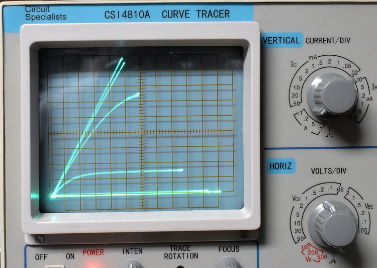
Picture showing an attempt to match two MPF102 FETs.
The above picture contains a mistake in the setup. I came just that far, thumb and for finger held a centimeter apart, from making an embarrassing phone call to Circuit Specialists customer support. When the LEFT and RIGHT radio buttons are pressed in sequence they show a family of curves with the bottom curve making the bottom line across the bottom of the screen as it should. When the DUAL button is pushed in, the two displays are elevated. Look at the locking button (in or out) switch that is located center and above the DUAL radio button. It is in the TRANS position instead of the FET position as it should have been for checking pairs of FETs for matching. If I had made that call to customer support they probably would have been polite enough not to call me a stupid ass but they would probably have wanted to. In any case I surely would have felt like one when they told me what I was doing wrong. Don't want to feel like a stupid ass? When matching transistors, either BJTs or FETs, be sure to put the push button switch in the correct position.
The photo below shows a pair of MPF102 FETs being compared. Finding exact matched pairs can be tedious but this curve tracer makes it a little easier. You still need a large number of devices and a generis helping of patients. The trace separation control can be used to move the two traces very close together but they won't move to the total overlap position. This may be due to a mistaken internal adjustment or a mistake on the part of the designers. To judge the most precise matching it would be necessary to have the two families of curves exactly overlaid.

Matching JFETs.
Matching BJTs.

Matching BJTs.
As with FETs, matching BJTs requires a stock of transistors and a generous supply of patients.
Holey parallax Batman! In the tracer I originally had, the graticule appeared to be etched into the inside of the screen in the manner of quality oscilloscopes made after about 1970. See any other photo except the one above. In this one the graticule is clearly outside of the CRT. What a bummer. I guess I had better get to work on those X and Y outputs for my DSO.
Tracing Tube Curves.
Note: While I negotiated with Circuit Specialists over returning the curve tracer I continued to work on the tube test fixture. That part of the tracer was functioning properly so I was able to continue working.Sometimes I wonder about the utility of a transistor curve tracer. There is so much variation from one to another of the same type number as to make a procedure such as load line analysis totally useless. On the other hand the few of us who are old enough to have been taught load line analysis in trade school or university know how powerful a tool it is in design of vacuum tube amplifiers. To that end I have built a tube test fixture. This is just the first of what is at present an unknown number.
Tube Test Fixture Mark I.
This is built using the 5E boards available from this website. These boards snap together. My first thought was to glue them but it seems that a glue that will really stick to plastic has yet to be invented. I was forced to use metal and screws as you can see in the pictures below.This fixture is made primarily to test dual triodes for matching. They are wired for the 12A_7 series but it appears that there was a defacto standard for dual triodes. Because there was some room left over I decided to add two 7 pin sockets for matching pairs of 6C4s. They could also be used to match pairs of any 7 pin tube including pentodes. This should be the only one of this size that I need to make.


Below you see the fixture mounted on the TEST SET. The 6 holes give access to the 6 pushbutton controls. There are a little small for a finger but the end of a nut driver is the perfect tool to push a button.
The color coding of wires from the dual triode socket is; Blue - Plate, Green - Grid, and Black - Cathode. Pin 9 comes out to the yellow jack on the front for parallel heater connection. I might change this later making it easier to trace a 9 pin tube other than a dual triode such as a triode - pentode. There's no law that says you have to exactly duplicate my version.
On the seven pin sockets the coding is by the numbers. Brown-1, Red-2, 5-Green, 6-Blue, and 7-violet. Pins 3 and 4 are wired to the two Green jacks on the front. The black and red jacks are for the purpose of feeding constant DC screen grid voltage making it possible to curve trace a tetrode or pentode. The black jack is wired to the TEST SET's ground through a modular connector so it can be changed if needed. The red jack is wired to a connector in the center of the board at the front.


Above you see the two families of curves for the two triodes in a 12AY7. In the picture below the TRACE SEPARATION control has been used to bring the two together. There is a slight mismatch between the two sections. Ideally both sets of curves should end at the same Y coordinates. Estimating matching would be a little easier if the designers had permitted the two traces to get much closer together if not exactly overlaid. This would have permitted each user to decide how close together he or she wanted them rather than imposing a limit decided by someone who is thousands of miles away.