Let me start this by telling you that I am not an expert on ferrite cores. I am now a retired software engineer who has always liked to tinker with electronics and simple mechanical things. I have taken far more things apart than I ever put together. Over the years, I used many computer systems that relied on ferrite core memories as their main memory. I have maintained a few of them and still own one, a Digital Equipment Corporation (DEC) PDP-8/S which is currently just stored in my garage.
In this article, I will tell you about something special that I discovered and explored many years ago. Around 1980 I bought an entire surplus magnetic core memory stack and set about trying to understand what I would have to do to make it work. As it turns out, I never did make it go and sold it to another experimenter but along the way, I discovered that it incorporated a most clever design for reducing the complexity and number of transistorized drivers needed to drive the core memory.
The core memory stack had been cut out of an IBM 1620 computer. Years earlier I had done a little programming on an IBM 1620 so I knew something of its general organization. This machine was of a decimal design. Its programming system and theory of operation was virtually unlike any machine running today. It viewed its main memory unit (that is, the core stack) as having 20,000 addresses. Each address could contain six bits. In that machine's view, four of those bits contained a decimal digit in binary-coded-decimal format. One more bit was called a Flag bit and served special purposes as an indicator. The remaining bit was coded as a parity bit which is a scheme for detecting memory failures. For our purposes here, we will just consider the computer as having run the memory as 20,000 addresses of six bit words.
In reality, the memory unit itself was actually organized as 10,000 addresses each of which contained a 12-bit word. I am sure it was a relatively straightforward design that made this appear to the rest of the machine as 20,000 addresses of six-bit words.
I am not going to describe here how core memory works in general as that can be found elsewhere. I will assume that the reader is already familiar with several concepts concerning magnetic core memory:
For the IBM 1620 main core stack, there are 100 X-wires and 100 Y-wires. The 100 X-wires and 100 Y-wires intersect at 10,000 locations in each bit plane of cores and there were 12 bit planes. The main core stack contained 120,000 individual small magnetic ferrite cores.
In most magnetic core memory designs, this type of core memory would have required 100 bidirectional X-wire drivers, 100 bidirectional Y-wire drivers, and 12 unidirectional drivers for the 12 inhibit wires. This would be a total of 212 driver circuits, most of which would have to been bidirectional. But the designers of this system worked out how to do the job using just 53 drivers and every one of them was a unidirectional driver.
For the moment, let us move the discussion to a different type of magnetic cores. These cores were once referred to as logic cores, switch cores, or BIMAG cores. Most were made of material very similar to that of the ferrite cores in core memories but the cores were much larger in size. I have seen these large cores be as large as about 1/2 inch in diameter. I have also seen some such cores that were constructed of a plastic bobbin with a ribbon of some shiny alloy wrapped many times around them. For our purposes here, I we will refer to these large cores as driver cores for reasons that will become apparent as we go along.
Because these cores are much larger, a wire is easily able to pass through one not just once as in an X/Y core memory array but with multiple turns. Such a wire may thus be thought of as a primary or secondary winding similar to that of a transformer. The big difference is that the core material has a high hysteresis. In an efficient transformer, high hysteresis is not what one wants. In any case, having many turns in a winding dramatically lowers the current required to switch the state of a core. In a secondary winding, having many turns increases the amplitude of the signal that is generated in the winding.
The reader might be interested in watching a pair of U.S. Army films that are available on YouTube. Each film is about 28 minutes in length. They were produced in 1961 and 1962. They describe details of circuits that can perform a lot of operations that we associate with data processing using only magnetic cores, pulse sources, and some diodes. For example, it is shown how shift registers can be made from just a few such parts.
MAGNETIC CORES PART I - PROPERTIES
MAGNETIC CORES PART II - BASIC CIRCUITS
In these videos, you will see that flipping a core can generate enough current in a secondary (or "sense" winding) to serve as the pulse into another winding of a second core and therefore flip the state of the second core.
This is how I remember the IBM 1620 core memory stack looked in general:
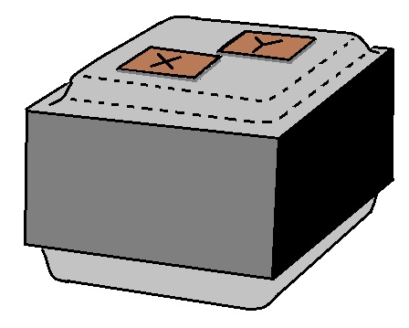
The unit was perhaps 12 or 14 inches square and about 14 inches tall. The sides were covered in little wire links (not shown) that interconnected the X and Y wires of adjacent horizontally oriented bit planes. On the top and bottom, there were gray plastic covers that bulged out as shown in the sketch above. On the top, there were two phenolic boards which are labeled in the diagram X and Y. The secret to the low driver count and the lack of a need for any bidirectional drivers lies in these two phenolic boards.
Each of theses boards contained a set of 100 of the large switch cores. These particular switch cores were about 1/4 inch in diameter and about 3/16 inch thick. They were arranged in a matrix on their boards, 10 rows by 10 columns.
In order to simplify the description of this system, let us consider instead a hypothetical core memory with only 256 8-bit words. We would typically expect that such a core memory would be arranged as 8 bit planes with each bit plane having 16 X-wires and 16 Y-wires. But rather than driving each X-wire and each Y-wire with a bidirectional driver, let us wind a secondary winding on a large switch core and use that to drive the X or Y wire.

If we flip the state of the X-Drive core in one direction, we induce a pulse of current through the associated X-wire in the stack. The same is true of the Y-Drive core. The induced pulse is brief. If the correct number of turns is used in the secondary winding of the X-drive core, the brief pulse can be of half enough current to change the state of any small memory core the X wire passes through. The same is true of the Y-drive core. If both the X-drive core and the Y-drive core change state at the same moment, the two half currents can set the state of every core they both pass through to one particular state which we can arbitrarily assign to be their zero state. In this case, there are eight such cores, one per bit plane.
Of couse, if we flip both the X-drive and Y-drive cores back to their original states, they will each generate a similar half current pulse again, but in the opposite direction. That will similarly set all eight small memory cores where their X- and Y-wires intersect back to their opposite state which we can assign to be their one state.
Remembering that there are actually 16 X-wires running through this 256 byte memory, we would need 16 of the large X-drive cores to drive them. Here is how they should be arranged:
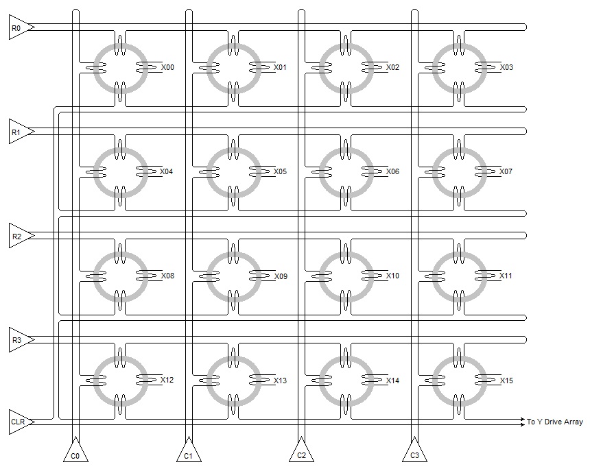
In this array of drive cores, we see that each core has a secondary winding leading off to the right. They are labelled X00, X01, X02, etc. Only this single winding of each drive core is driven by magnetic flux changes in the drive core. Each of the other three windings is driven by a unidirectional driver. The top winding of each core in a row is connected in series so that a pulse driven by a row driver (such as R0, R1, R2, or R3) attempts to magnetically set every core in that row. Similarly, windings shown along the left side of the cores are interconnected so that each column driver (C0, C1, C2, or C3) can attempt to magnetically set every core in its column. However, the magnetic flux generated by any of these windings through the drive cores is insufficient to change the state of a drive core except where a driven row and a driven column in the drive core array intersect. Just like the small cores of the main core stack, these drive cores are addressed and set by the intersection of two half currents.
There remains one more driver. Located in the lower left corner of the diagram, it is labelled CLR. For the moment, assume the two wires shown exiting the right side of the diagram to the Y Drive Array are simply shorted together. After one drive core has been magnetically set as described above, the CLR driver outputs a pulse of current that is sufficiently strong to reset any core through which it passes. Rather than being a pulse of half current, it is a pulse of full current. The CLR wire passes through every core in the entire drive core array. Since only one drive core is set, only that one drive core gets reset.
Those two wires that are shown exiting the X drive core array diagram to the Y Drive Array actually go to the CLR winding in the duplicate array of drive cores for the Y Drive Array. That is, there is only one CLR driver and it serves both drive arrays. In all other respects, the X and Y drive core arrays are identical in construction.
Now we direct our attention to the read and write cycles of the entire core memory system. To read the contents of the eight cores in one of the 256 addresses of the main core array, we need a half current pulse in one direction on a particular X-wire and another half current pulse in the corresponding direction of a particular Y-wire. By simultaneously pulsing one of the row drivers in the X drive core array, one of the column drivers in the X drive core array, one of the row drivers in the Y drive core array, and one of the column drivers in Y drive core array, one drive core in each array is set, inducing a half current pulse in one X-wire and one Y-wire in the main core stack.
The eight cores where those half currents intersect are each cleared. For any of them that were previously set, a small pulse is induced in the sense winding in that small core's bit plane. Each sense amplifier detects whether a pulse was induced and the amplified results are set into a memory data register.
Since the read cycle was destructive, we now either wish to rewrite that same data back into the same cores from where it was read or to write new data into those same cores. Either way, we need a half current pulse in the opposite direction on the same X-wire and the same Y-wire as before. All we need to do is pulse the single CLR driver. Its only effect is to clear whichever drive core was set in the X drive core array as well as whichever drive core was set in the Y drive core array. The result is a half current pulse as before (but in the opposite direction) on the same X-wire and the same Y-wire as was used during the destructive read cycle.
Since these two half currents would result in every core of the addressed byte being written to a one, an inhibit wire is provided in each bit plane. During the write operation, for each bit that is to remain a zero during the write operation, the corresponding inhibit wire is pulsed with a counter half current to prevent any core in its bit plane from becoming a one.
Amazingly, every driver in the entire system has only to drive current through its output wire in but one direction.
Returning now to the IBM 1620 core memory stack, the X drive core array and the Y drive core array on top of the unit each contained 100 drive cores, arranged as 10 rows by 10 columns. Therefore, the system needed only 40 drivers for rows and columns of the drive core arrays plus a single CLR driver. Add the 12 inhibit drivers for the 12 bit planes and you have the total of 53 drivers and all are unidirectional.
There was another odd thing about the IBM 1620 computer. When you powered it up, you had to wait for something like ten minutes before you could use the machine. The machine just sat there with the power on in a standby mode while its human operators wondered why it took so long to "warm up". As it turns out, warming up is exactly what it was doing.
Soon after the IBM 1620, more modern computers that used core memory included some type of temperature sensing device in the core stack. It seems that the small ferrite memory cores are temperature sensitive. The amount of current produced by the drivers must vary according to how warm the memory cores are. In the IBM 1620 that was accomplished by intentionally warming the cores to a known fixed operating temperature before attempting to use them. Under the gray plastic covers on the top and bottom of the core stack, there was an electric fan for circulating the air inside, an electrical heating element, and a simple fixed thermostat. When the IBM 1620 was powered up, it stayed in standby mode until the core stack was up to the intended temperature which was well above room temperature.
Comments or questions? Send them to: