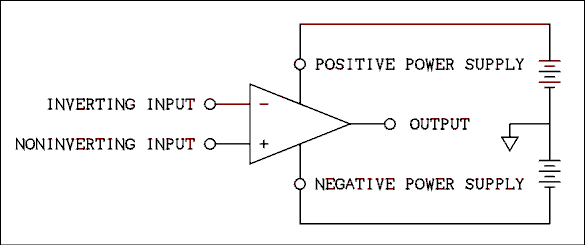
Figure 6.1 Operational Amplifier Showing Power Supply Connections.
For a verbal description click here.
Chapter 6 The Operational Amplifier.
6.1 Op Amp Behavior.
6.2 Equations of the Op Amp.
6.3 The Unity-Gain Buffer Amplifier.
6.4 The Noninverting Amplifier.
6.5 The Inverting Amplifier.
6.6 The Summing Amplifier.
6.7 The Integrating Amplifier.
6.8 Single Power Supply Operation.
6.9 Understanding Op Amp Specifications.
6.10 Problems.
6.11 Answers to Problems.
Chapter 6
The Operational Amplifier.
The operational amplifier began life as a component in an analog computer. For those who have never heard of an analog computer, it is (was) a computer in which the magnitude and sign of voltages were used to represent physical quantities. For example, one voltage might represent the velocity of a falling object, another voltage the acceleration and another voltage might represent the frictional drag of the air on the object. If you know about analog computers you think of them as being vacuum tube monstrosities but that is because of the age in which they were developed and used. If they were still in use today they would be reduced in size to desktop or even smaller just as their more successful digital brothers have.The operational amplifier (op amp) is so called because in its original application it was used to perform mathematical operations. The two operations it was best at were addition and integration. Op amps are still used for these purposes but they have found many other applications in modern electronics.
Back to Fun with Transistors.
Back to Fun with Tubes.
Back to Table of Contents.
Back to top.
6.1 Op Amp Behavior.
The op amp has been reduced from its original vacuum tube size of a cubic foot or larger to an 8 pin integrated circuit. There are several hundred different type numbers, each having its own particular and sometimes subtle difference from others. The internal circuitry of these ICs is not terribly important to us. IC manufacturers do not often give the internal circuit diagrams of their ICs. Op amps are among the few exceptions to this rule.The circuits are quite complex, the 741 op amp has 20 transistors in it. The curious student is referred to instructional books and data books devoted exclusively to op amps. There are many such books available.
Op amps are usually treated as 5 terminal devices. In the following pages they will be treated as just another component the same as a transistor is a component.
Electrical Connections.
The op amp has 5 basic electrical connections. They are inverting input, noninverting input, output, positive power supply and negative power supply. While there is no ground per se, ground is established by the power supply. Employing the theorem which states that "one picture is worth a thousand words" refer to Figure 6.1. The power supplies are replaced by batteries to make it clear how the power supplies are connected. Sometimes an op amp may be operated from a single power supply but most of the time they are operated as shown in Figure 6.1.Except for section 6.8 you will not again see the power supply connections to an op amp. The power supply connections are always there; they are usually not shown on schematic diagrams. The op amp will not work without power supply connections. If you see a diagram which does not show power supply connections and you assume that it is not necessary to connect a power supply, you will be in error. The op amp will not work without power supply connections. They are always assumed if not shown.

Figure 6.1 Operational Amplifier Showing Power Supply Connections.
For a verbal description click here.
The two inputs must be at a voltage which is between the negative and positive power supplies. To force the voltage of either or both inputs higher than V+ (the positive power supply) or lower than V- (the negative power supply) may destroy the op amp. (There are some special purpose op amps which have been designed to permit the inputs to be at potentials outside of the power supplies. If you have a need to set the inputs outside of the power supplies, you should consult a data book to find such an op amp.)Many op amps have inputs for adjusting the offset voltage to zero. When the voltage at the two inputs is exactly equal the output should be zero but it is not. The amount by which the input voltage must be different to bring the output to zero is the offset voltage.
The Differential Inputs.
If the inverting input is tied to ground and a variable DC voltage is applied to the noninverting input the output will go with the sign of the noninverting input. If the voltage at the noninverting input is positive, the output is positive and if the voltage at the noninverting input is negative, the output is negative.Now we will disconnect the inverting input from ground and connect the noninverting input to ground. The variable DC voltage will be applied to the inverting input. When the voltage at the inverting input is positive, the output voltage is negative. When the voltage at the inverting input is negative, the output voltage is positive. Thus you can see why the inputs have been named as they have.
Theoretically, if both inputs are connected together, the output voltage is zero. The offset adjustments can be used to adjust the output to zero, but there is a little more to it than that. If the two inputs (tied together) are made positive or negative, the output voltage will not change. But that's only in theory.
In practical op amps the output voltage will change a little when the two inputs have the same voltage applied to them. A voltage which is applied to both inputs simultaneously is called a common mode voltage. A voltage which is applied between the two inputs is called the normal mode voltage or differential voltage.
The normal mode gain is defined as the ratio of output voltage to the differential input voltage.
ANM = VO / Vd (6.1) Where VO is the output voltage and Vd is the voltage difference between the two inputs. The common mode gain is defined as the ratio of the output voltage to the common mode input voltage.ACM = VO / VCM (6.2) Where VCM is the voltage applied to both inputs together. The common mode rejection ratio is defined as the ratio of the normal mode gain to the common mode gain.CMRR = ANM / ACM (6.3) The common mode rejection ratio (CMRR) is usually expressed in dB. The typical value for the 741 type op amp is given as 90 dB.Example 6.1.
An op amp has had its offset adjusted to zero. Its inverting input is at +3.001 v and its noninverting input is at +3.000 v. Will its output be positive or negative?Solution:
The noninverting input is negative with respect to the inverting input; therefore, the output will be negative.Example 6.2.
An op amp has had its offset adjusted to zero. Its inverting input is at -5.001 v and its noninverting input is at -5.000 v. Will its output be positive or negative?Solution:
The noninverting input is positive with respect to the inverting input; therefore, the output will be positive.Example 6.3.
When the normal mode voltage is changed by 25 uv the output changes by 5 volts. When the common mode voltage is changed by 1 volt the output voltage changes by 6.325 volts. (a) What is the CMRR? (b) Express the CMRR in dB.Solution:
The normal mode gain is 5 v / 25 uv = 200,000. The common mode gain is 6.325 v / 1 v = 6.325. (a) The CMRR is 200,000 / 6.325 = 31620. (b) The CMRR expressed in dB is 20 LOG (31620) = 90 dB.Back to Fun with Transistors.
Back to Fun with Tubes.
Back to Table of Contents.
Back to top.
6.2 Equations of the Op Amp.
The equation of the op amp is based on an approximation, albeit a very good one. Let us restate the feedback equation.A' = A / (1 + A beta) (6.4) Now we will find the limit as A approaches infinity. If we divide both numerator and denominator by A we haveA' = 1 / (1/A + beta) (6.5) As A approaches infinity, the 1/A term goes to zero leavingLimit as A approaches infinity of A' = 1 / beta (6.6) Thus, the gain of an op amp with feedback applied is given byA' = 1 / beta (6.7) While equation 6.7 is a very good approximation in most cases it should not be taken as gospel.Example 6.4.
An op amp has a DC gain of 100,000 and a unity gain bandwidth of 1 MHz. If feedback is applied to the op amp with a beta value of 0.05, what is the exact closed-loop gain at (a) DC, (b) 1 kHz, (c) 20 kHz, and (d) 100 kHz?Solution:
From equation 5.15.5 the corner frequency is,fc2 = fhu / AMax
Where fc2 is the corner frequency, fhu is the upper unity gain frequency, and AMax is the DC gain.
fc2 = 1 MHz / 100,000 = 10 Hz.
(a) Using equation 6.4,
A' = A / (1 + A beta) = 100,000 / (1 + 100,000 x 0.05) = 19.9960
(b) Using equation 5.4.1
A' = ADC / sqrt([f / fc2]2 + [1 + ADC beta]2)
A' = 100,000 / sqrt([1,000 / 10]2 + [1 + 100,000 x 0.05]2) = 19.9920
(c) and (d) also use equation 5.4.1.
(c) A' = 18.5663
(d) A' = 8.94391
Example 6.5.
For the conditions of example 6.4 calculate the percent error of gain using 1/beta as the standard of comparisons at (a) DC, (b) 1 kHz, (c) 20 kHz, and (d) 100 kHz.Solution:
Since 1/beta = 20.00000 the errors are as follows:As can be seen from these examples the 1/beta approximation is very good at DC and low frequencies but somewhere between 1 and 20 kHz the error crosses over the 2% line. If it is desired to know the exact gain at high audio frequencies equation 5.4.1 must be used rather than 6.4 or 1/beta.(a) -0.020%, (b) -0.040%, (c) -7.1685%, (d) -55.2805%.
Back to Fun with Transistors.
Back to Fun with Tubes.
Back to Table of Contents.
Back to top.
6.3 The Unity-gain Buffer Amplifier.
The definition of a buffer amplifier is an amplifier which will isolate a load from a source. Such isolation usually requires that the buffer amplifier have a very high input impedance. The output impedance may either be very low or matched to the load impedance. A buffer often has unity voltage gain although this is not a requirement under the definition.A unity gain buffer has a voltage gain of unity as the name implies. The value of beta is set at unity by feeding back all of the output voltage to the inverting input. The circuit of Figure 6.2 is of a unity gain buffer.

Figure 6.2 Unity Voltage Gain Buffer Amplifier.
For a verbal description click here.
An op amp works by adjusting its output so that the two inputs are at the same potential. (The error due to finite op amp gain is quite small.) Because the output and the inverting input are connected together the output voltage will be the same as the inverting input voltage. Suppose that the input voltage is 0 volts and that the voltage is suddenly changed to +2 volts. Since the signal is applied to the noninverting input, for an instant of time the noninverting input will be positive with respect to the inverting input. This will cause the output to go positive. When the inverting input voltage becomes +2 volts the output will stop changing. Should the output voltage overshoot +2 volts and become higher, the output would be urged in the negative direction thus correcting the overshoot. A properly compensated op amp will not overshoot in the first place.The voltage at the output cannot become 2.000000000000 volts. If it did the differential input voltage would be zero and the output would be zero. Since the output voltage is finite, there must be a finite difference in voltage between the noninverting input and the inverting input. That small but finite difference is caused by the finite open-loop gain of the op amp. Because the open-loop gain of the op amp is very large, the error is very small.
The percent error is,
% error = 100% x (Measured - Reference) / Reference (6.8) If we substitute A / (1 + A beta) for "Measured" and 1/beta for "Reference" in equation 6.8 and get some more algebraic exercise we have% error = -100% / (1 + A beta) (6.9) In the case of the unity-gain buffer the value of beta is 1.0000000000; therefore, the % error becomes 100% / (A + 1).Example 6.6.
Calculate the gain error of a unity-gain buffer if the op amp has an open-loop gain of (a) 200,000; (b) 20,000; (c) 1,000; and (d) 20?Solution:
The % error is (a) -100% / (1 + 200,000) = -0.0004999975%, (b) -0.00499975%, (c) -0.0999%, (d) -4.7619%.The closed-loop input and output impedances of the unity-gain buffer are,ZIN' = ZIN (1 + A beta) (6.10) AndZO' = ZO / (1 + A beta) (6.11) The open-loop input and output impedances must be obtained from an IC data-book. Because beta is unity and the open-loop gain is very large, the output impedance is very low and the input impedance is very high.Often it is desired to calculate the input and/or output impedance at higher frequencies where the gain is less than the DC gain. Equations 6.10 and 6.11 may be used but the value of A must be the gain at the frequency being considered, not the gain at DC. This gain can be obtained from equation 5.15.1 which is repeated below.

Where A is the gain at any frequency, ADC is the DC gain of the amplifier, f is the frequency at which the gain is desired, and fc2 is calculated from equation 5.15.5 which is repeated below.fc2 = fhu / ADC (6.11.2) Where fhu is the unity gain bandwidth or gain bandwidth product of the amplifier.Example 6.7.
Determine the minimum input impedance and the maximum output impedance of a unity-gain buffer employing a type 741 op amp. The data book gives the minimum input resistance of the 741 as 0.3 M ohms, a typical output resistance of 75 ohms and a minimum gain of 20,000. The typical gain is given as 200,000.Solution:
The minimum gain is given as 20,000. The typical gain is given as 200,000 but as the question asks for the minimum input impedance and maximum output impedance, the minimum gain should be used.The resistance of the printed circuitboard traces will be greater than the output resistance of the amplifier. Note also that this is a worst case. If the typical gain of 200,000 had been used, the input impedance would be 60 G ohms and the output impedance 0.375 m ohms.ZIN = 0.3 M ohms x 20,000 = 6 G ohms,
The output impedance is, ZO = 75 / 20,000 = 3.75 milli ohms.
Back to Fun with Transistors.
Back to Fun with Tubes.
Back to Table of Contents.
Back to top.
6.4 The Noninverting Amplifier.
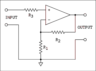
Figure 6.3 Noninverting Amplifier.
For a verbal description click here.
The circuit of a noninverting amplifier is given in Figure 6.3. As we saw in the previous chapter the value of beta for this amplifier is given by,beta = R1 / (R1 + R2) (6.12) The approximation for the closed-loop gain is given by equation 6.7. If the gain error is large, equation 6.4 should be used to calculate the exact gain. The gain error is given by equation 6.9. The input and output impedances are given by equations 6.10 and 6.11.This circuit works because the op amp will always adjust its output until both inputs have the same potential. If a given potential is placed between the input terminals in Figure 6.3 the noninverting input of the op amp will be placed at that potential. The op amp will adjust its output until the inverting input is at the same potential. Because of the voltage divider consisting of R1 and R2 the output voltage must be greater than the input voltage by the amount of the divider ratio. The conditions of equal potential at both inputs require that they have the same sign. Because resistors can't change the sign of a voltage, the output voltage must also have the same sign as the input voltage.
Example 6.8.
A noninverting amplifier has the following values: R1 = 4.7 k ohms and R2 = 2.7 k ohms. The open-loop gain is 200,000. What is the closed-loop gain?Solution:
When the open-loop gain is very high the closed-loop gain is 1/beta. Therefore, the closed-loop gain is given by A' = (R1 + R2) / R1 = (4.7 k ohms + 2.7 k ohms) / 4.7 k ohms = 1.57.Example 6.9.
A noninverting amplifier is to have a gain of 20 dB and R2 is to be a 10 k ohm resistor. What is the necessary value of R1?Solution:
The first step is to convert dB into gain.A' = 10dB/20 = 1020/20 = 101 = 10.
Since A' = 1/beta to obtain a gain of 10, beta must equal 0.1. Solving equation 6.12 for R1 gives,
R1 = beta R2 / (1 - beta)
R1 = 0.1 x 10 k ohms / (1 - 0.1) = 1.11 k ohms.
Back to Fun with Transistors.
Back to Fun with Tubes.
Back to Table of Contents.
Back to top.
6.5 The Inverting Amplifier.
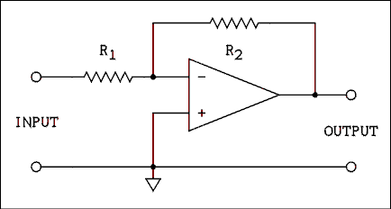
Figure 6.4 Inverting Amplifier.
For a verbal description click here.
The circuit of an inverting amplifier is given in Figure 6.4. As we saw in the previous chapter the value of beta for this amplifier is given by,beta = R1 / R2 (6.13) The approximation for the closed-loop gain is given by equation 6.7. If the gain error is large, equation 6.4 should be used to calculate the exact gain. The gain error is given by equation 6.9. The input impedance is given by,RIN = R1 (6.14) The output impedance is given by equation 6.11.This circuit also works because the op amp will always adjust its output until both inputs have the same potential. If a voltage of a given sign and magnitude is placed between the input terminals in Figure 6.4 the inverting input of the op amp will be placed at a potential which is determined by R1 and R2. The op amp will adjust its output until the inverting input is at the same potential as the noninverting input. Because the noninverting input is grounded, the inverting input will always be adjusted to zero potential. Figure 6.5 shows an equivalent circuit to the inverting amplifier.
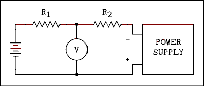
Figure 6.5 Equivalent Circuit of an Inverting Amplifier.
For a verbal description click here.
Imagine that you are watching the voltmeter and adjusting the voltage of the power supply. If the polarities are as shown, you will be able to find a voltage at which the voltmeter reads zero. At this point the voltmeter current will be zero and the current in R1 equals the current in R2. If the battery is VIN and the power supply is VO thenVIN / R1 = VO / R2. (6.15) Therefore, we can write,VO / VIN = R2 / R1. (6.16) In order to bring the voltage across the voltmeter to zero, VIN and VO must have opposite signs. The op amp does exactly the same thing. The voltmeter is replaced by the input and the power supply is replaced by the output of the op amp. The op amp will adjust its output until the voltage between the two inputs is zero. When this has been accomplished, equations 6.15 and 6.16 will be satisfied.Example 6.10.
An inverting amplifier has the following values: R1 = 4.7 k ohms and R2 = 2.7 k ohms. The open-loop gain is 200,000. What is the closed-loop gain?Solution:
When the open-loop gain is very high the closed-loop gain is 1/beta. Therefore, the closed-loop gain is given by,A' = R2 / R1 = 2.7 k ohms / 4.7 k ohms = -0.574.
That's right. It's possible for an inverting amplifier to have a gain of less than unity.
Example 6.11.
An inverting amplifier is to have a gain of 30 dB and R2 is to be a 10 k ohm resistor. What is the necessary value of R1?Solution:
The first step is to convert dB into gain.A' = 10dB/20 = 1030/20 = 103/2 = 31.62.
Since A' = 1/beta, to obtain a gain of -31.62, beta must equal 0.03163. Solving equation 6.13 for R1 gives,
R1 = beta R2 = 0.03163 x 10 k ohms = 316 ohms.
Back to Fun with Transistors.
Back to Fun with Tubes.
Back to Table of Contents.
Back to top.
6.6 The Summing Amplifier.
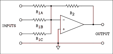
Figure 6.6 Summing Amplifier with Three Inputs.
For a verbal description click here.
The circuit of a summing amplifier is given in Figure 6.6. Remember that the op amp will adjust its output so that the voltage at the inverting input will be zero. Thus the current flowing in R2 must be the sum of the individual currents in R1A, R1B and R1C. The output voltage is given by,VO = R2 [VINA / R1A + VINB / R1B + VINC / R1C] (6.17) A very good way to solve problems involving circuits of this kind is to treat them as circuit analysis problems.Example 6.12.
In a circuit similar to that of Figure 6.6 the values are as follows: R1A = 10 k ohms, R1B = 7.5 k ohms, R1C = 5 k ohms, R2 = 10 k ohms, VINA = +15 v, VINB = -9 v, and VINC = -8 v. What is the output voltage of the amplifier?Solution:
We will sum the currents at the node where the 4 resistors are joined. This node is at zero potential.The point where all of the resistors connect, (the inverting input), is often called the summing node or the summing junction. As has been said many times, this point is at zero potential. Of course it is not truly at zero potential because the amplifier does not have infinite gain. In most cases the gain of the amplifier is so high that the summing node is virtually at ground potential. The summing node is said to be a virtual ground point. It behaves as if it were actually shorted to ground.IA + IB + IC = I2.
Let us define current into the node as positive.
IA = VINA / R1A = 15 v / 10 k ohms = 1.5 mA.
IB = -9 v / 7.5 k ohms = -1.2 mA.
IC = -8 v / 5 k ohms = -1.6 mA.
I2 = 1.5 mA -1.2 mA -1.6 mA = -1.3 mA.
The net current flows out of the node; therefore, I2 must flow into the node to prevent a charge imbalance in the conductors. The current in R2 is flowing to the left, which means that the right end is positive with respect to the summing node. The voltage across R2 is I2 R2 = 1.3 mA 10 k ohms = +13 volts. Equation 6.17 will give the same answer.
Example 6.12 illustrates that a summing amplifier gives the negative of the true sum of the input voltages. This was one of the original uses of an operational amplifier.
Although we are not sound engineers, most of us own stereo systems and examples from that field are easy to relate to and understand. Suppose it is desired to add together the left and right channels of a stereo signal to form a monaural signal for a monaural amplifier. At the same time it is necessary to maintain the individual integrity of the left and right signals to feed a stereo amplifier. A circuit similar to Figure 6.6 but with two equal value resistors in the inputs will do the job nicely. The output will be a true L + R sum which is required for a monaural image. Because the summing node is a virtual ground, the individual L and R signals will not get mixed up in the lines before the summing amplifier. Audio engineers call this circuit a mixer but radio engineers mean something completely different when they say "mixer". Our best course is to avoid the term all together.
Back to Fun with Transistors.
Back to Fun with Tubes.
Back to Table of Contents.
Back to top.
6.7 The Integrating Amplifier.

Figure 6.7 Integrating Amplifier.
For a verbal description click here.
The other original use of an operational amplifier was as an integrator. An integrator is an electronic circuit which takes the time integral of any function which has been converted into a time varying voltage and applied to the input of the circuit. As you can see in Figure 6.7 the feedback resistor has been replaced by a capacitor. In a real circuit there is a switch in parallel with the capacitor to be certain that it starts out with zero initial charge.The op amp will adjust its output to keep its two inputs at the same potential. Since the noninverting input is grounded, the inverting input will also be at ground potential. The current in R is
i = vin / R. (6.18) The voltage across a capacitor is given by

The current in the resistor and the current in the capacitor are flowing in the same direction (left to right or right to left) and the connect point (summing node) is at zero potential. The voltage at the right end of the capacitor must have the opposite sign as the input voltage. If we substitute equation 6.18 into equation 6.19 and insert the negative sign required by the op amp we have

Now you will learn what an integral really is. Maybe you think you already know. Let's see if you do.Example 6.13.
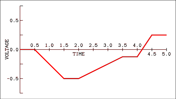
In Figure 6.7 the capacitor starts out with zero initial charge. The input voltage is as shown in Figure 6.8. Draw the output voltage versus time, giving scale values. R = 2 M ohms and C = 1 uf.Solution:
The integrator's output is shown in Figure 6.9. For the first 1/2 second there is no input and the output does not change. From 0.5 to 1.5 seconds the input voltage is 1.0 volts. That is an area of 1.0. If the gain of the integrator were unity, the output would be -1 after 1.5 seconds but this one has a 2 M ohm resistor which makes the 1/RC term in front of the integral to be 1/2. The input is 1 volt for 1 second or 1 volt second. The output will change by -0.5 volts/second for 1 second to give a value of -0.5 volt. From 1.5 seconds to 2.0 seconds the input is zero and the output will not change. Notice that the output is not zero when the input is zero. When the input is zero there is no additional area being added to the integral and so the output simply stays where it is. The input is -0.5 volts from 2 to 3.5 seconds which is an enclosed area of 0.75. Because of the gain of the integrator the output will change by +0.375 volts during the 1.5 seconds when the input is -0.5 volts. The output voltage will change at a rate of 0.25 volts/second for 1.5 seconds. At the end of 3.5 seconds the output will be -0.125 volts. The output will remain at this level from 3.5 to 4.0 seconds when the input is zero. When the input goes to -1.5 volts the output will change at a rate of 0.75 volts/second for a time of 0.5 seconds. The enclosed area is 0.75 and so the output will change by an amount of 0.375 volts. The output will end up at a voltage of +0.25 volts. The output will remain at this level until there is additional input or the capacitor is discharged. There is no requirement that the output come back to zero.
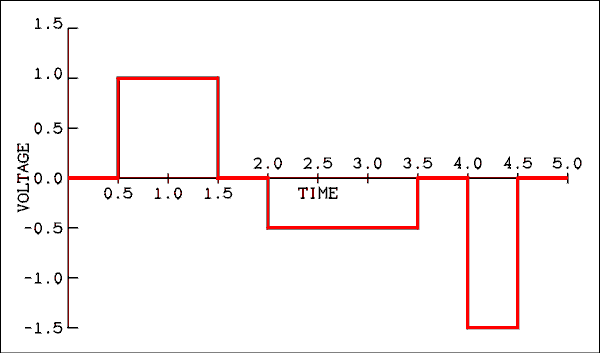
Figure 6.8 Integrator Input Voltage Versus Time.
For a verbal description click here.
Figure 6.9 Output Voltage of an Integrator.
For a verbal description click here.
Integrating amplifiers were used in analog computers to solve differential equations. They still can be used for that but digital computers will do it with more accuracy.Back to Fun with Transistors.
Back to Fun with Tubes.
Back to Table of Contents.
Back to top.
6.8 Single Power Supply Operation.
The major advantage of operating op amps from two power supplies is that the input to and output from the op amp can be positive or negative. Because the input voltage can be zero, slowly changing DC voltages may be amplified, added or integrated.In some applications it may not be necessary to have a bipolar output or the signals to be processed may be AC only. In such a case it is best to power an op amp from a single power supply. One power supply is less costly, smaller, lighter and generates less heat than two power supplies.
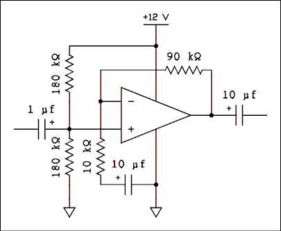
Figure 6.10 Single Power Supply Noninverting Amplifier.
For a verbal description click here.
Figure 6.10 is the circuit of a noninverting amplifier with a gain of 10 which operates from a single power supply. The parts which distinguish this circuit from a dual power supply amplifier are the two 180 k ohm resistors in the noninverting input circuit and the capacitors in the input, output and feedback portions of the circuit. The purpose of the 180 k ohm resistors is to bias the noninverting input at 1/2 of the power supply voltage. The values given are typical for an op amp with BJT inputs. The only DC path to the inverting input is through R2 from the output of the op amp. For best temperature stability the parallel combination of the biasing resistors should equal R2. This makes the DC Thevenin resistance in both inputs the same. If an FET input op amp were used the resistors could be as high as 10 M ohms each. The only requirement is that they be equal. The capacitor in the input prevents the circuit which is connected to the input from disturbing the bias on the noninverting input. Because the op amp always makes its two inputs have the same potential, the inverting input will also be at 1/2 the power supply and so the capacitor which is in series with the 10 k ohm resistor in the feedback network prevents this voltage from being disturbed. This capacitor has the additional effect of reducing the gain to unity for DC.

Figure 6.11 Single Power Supply Inverting Amplifier.
For a verbal description click here.
Figure 6.11 shows an inverting amplifier which will operate from a single power supply. This amplifier has a gain of -10. Once again the noninverting input is biased by a pair of equal value resistors to set its voltage at 1/2 of the power supply. Once again the parallel combination of the two biasing resistors should equil R2. The capacitor at the input is necessary to prevent upsetting the voltage at the inverting input.There are some special purpose op amps which are designed for single supply operation. Their inputs may be placed at or even a little below ground even though the op amp is operating on a single positive power supply. However, the output of such an op amp can only have potentials of ground + 1.2 volts to VCC -1.2 volts. For best operation an offset should be added to the input to place the output at 1/2 of VCC.
Back to Fun with Transistors.
Back to Fun with Tubes.
Back to Table of Contents.
Back to top.
6.9 Understanding Op Amp Specifications.
To the uninitiated an op amp specification sheet can be a bit bewildering. The table of specifications has columns for minimum, typical and maximum values. Few entries in the table have values under all three columns. Also there are numerous footnotes giving the conditions under which the parameter was measured. Such things as power supply voltage, load resistance, source resistance and ambient temperature can all affect the value of any given parameter.Input Offset Voltage is the voltage which must be applied to the input terminals to bring the output exactly to zero. The typical and maximum values are given here. The untrimmed value is given, which means that no trimmer pot was connected to the pins provided for that purpose. The units are usually mV (the units are always stated in the table).
Input Bias Current is the current which flows into each input of an op amp. If the input stage is a pair of BJTs, the base current of the transistors is the bias current. If the input is a pair of FETs, the bias current is the leakage current of the P-N junction which makes up the gates of the FETs. The units may be uA, nA or pA depending on the op amp. This specification is only significant when the resistance in series with the inputs is large. If the source resistance is such that the voltage drop due to the input offset current is significant compared to the input offset voltage, the resistance in the two inputs must be equal.
Input Offset Current is the difference between the bias currents in the two inputs. If the input bias current is producing a significant drop across the source resistances, the offset current will be converted to an offset voltage by the IR drop across the source resistances.
Input Resistance is the resistance the op amp inputs present to an input signal without any feedback applied to the amp.
Input Capacitance is the effective capacitance from each input to ground including Miller capacitance.
Offset Voltage Adjustment Range is only given on op amps which have pins for an offset voltage trimmer. It indicates how large the offset can be and still be adjusted to zero.
Input Voltage Range tells how far the inputs may be moved around in potential. This is usually the voltage which the amplifier will tolerate without damage. The input voltage range for proper operation of the amplifier may be given separately as a common mode voltage rating. It is usually 2 or 3 volts less than the maximum input voltage.
Common Mode Rejection Ratio (CMRR) is the ratio of normal mode gain to common mode gain. CMRR is most often given in dB. It is defined in detail on pages 244 and 245 of this text.
Supply Voltage Rejection Ratio states how much the power supply voltage will affect the output voltage of the op amp. It is the change in power supply voltage in uV divided by the change in output voltage in volts. This parameter is measured under open-loop conditions.
Large Signal Voltage Gain is the open-loop gain.
Output Voltage Swing states over what range the output voltage can vary.
Output Resistance is the Thevenin resistance of the amplifier.
Output Short Circuit Current states how much current will flow if the output of the amplifier is shorted to ground. Most op amps have built-in current limiting to protect them from damage if a short occurs.
Supply Current is how much current the op amp will draw from the power supply.
Power Consumption is the supply current multiplied by the total power supply voltage.
Transient Response (Unity Gain) states the risetime and overshoot for a unity-gain amplifier with a step input voltage.
Slew Rate is very important because it does more to limit the upper frequency limit than does the unity gain bandwidth. It states how fast the output voltage can change and is usually given in V/us.
The Gain Bandwidth Product or Unity Gain Frequency may be given in a graph rather than in the data table. It is the frequency at which the gain is unity.
Op amp data usually contains a large number of graphs. The majority of these graphs show how various parameters are effected by temperature. If you are going to use an op amp under conditions of extreme temperature, you should not ignore these graphs. If you are looking for a particular specification and it is not in the table, it may be in the graphs.
Back to Fun with Transistors.
Back to Fun with Tubes.
Back to Table of Contents.
Back to top.
6.10 Problems.
- A differential amplifier has a gain of 2.00, its noninverting input is at a potential of -1 volt and its inverting input is at a potential of +2 volts. What is its output voltage?
- A differential amplifier has a gain of 2.00, its noninverting input is at a potential of -5 volt and its inverting input is at a potential of -7.5 volts. What is its output voltage?
- A differential amplifier has a gain of 2.00, its noninverting input is at a potential of +7.5 volt and its inverting input is at a potential of +5 volts. What is its output voltage?
- When the normal mode voltage is changed by 30 uv the output changes by 4.5 volts. When the common mode voltage is changed by 1 volt the output voltage changes by 4.7434 volts. (a) What is the CMRR? (b) Express the CMRR in dB.
- An op amp with a DC gain of 200,000 and gain-bandwidth product of 1 MHz is being used in a unity-gain buffer. What will be the gain error at a frequency of 200 kHz?
- An op amp with a gain-bandwidth product of 1 MHz is being used in a unity-gain buffer. The input impedance is 500 k ohms. Over what range of frequencies will the buffer have an input resistance in excess of 10 M ohms? The DC gain is 200,000.
- A noninverting amplifier similar to Figure 6.3 has the following values: R1 = 1 k ohm and R2 = 13 k ohms. What is the DC gain of this amplifier?
- A noninverting amplifier is to have a gain of 12.00 and R1 is to be a 2.0 k ohm resistor. What is the value of R2 which will give the desired gain?
- A noninverting amplifier is to have a gain of 5 dB. The series combination of R1 and R2 must be greater than 2 k ohms but the parallel combination must not exceed 10 k ohms. Select standard 5% resistor values to come as close as you can to a gain of 5 dB and remain within the requirements stated. State the resistors you selected and the actual gain in dB which these values will produce.
- An inverting amplifier similar to Figure 6.4 has the following values: R1 = 1 k ohm and R2 = 13 k ohms. What is the DC gain of this amplifier?
- An inverting amplifier is to have a gain of 12.00 and R1 is to be a 10 k ohm resistor. What is the value of R2 which will give the desired gain?
- An inverting amplifier is to have a gain of 15 dB. The value of R2 must be greater than 2 k ohms but the parallel combination of R1 and R2 must not exceed 10 k ohms. Select standard 5% resistor values to come as close as you can to a gain of 15 dB and remain within the requirements stated. State the resistors you selected and the actual gain in dB which these values will produce.
- In a summing amplifier R1A = R1B = R1C = R2. Input A is 2 volts, input B is 3 volts and input C is -1 volt. What is the output voltage of the summing amplifier?
- In an integrator the resistor is a 1 M ohm and the capacitor is a 0.5 uf. The input to the integrator is as shown in Figure 6.12. Draw the graph of the output voltage versus time.
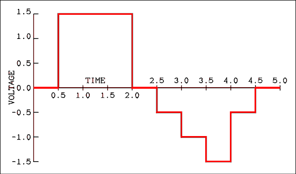
Figure 6.12 Input Voltage for Problem 14.
For a verbal description click here.
- An op amp has an input offset voltage of 1.5 mV, an input bias current of 0.2 uA and an input offset current of 0.03 uA, all typical values. Assuming equal resistances in series with each input, what is the maximum resistance for the voltage due to the input offset current to equal the input offset voltage?
- The input bias current is probably the most temperature sensitive of all op amp parameters. In an inverting amplifier the value of R1 is 47 k ohms and R2 is 120 k ohms. What resistor should be placed in series with the noninverting input to minimize the effects of temperature on the operating point?
Back to Fun with Transistors.
Back to Fun with Tubes.
Back to Table of Contents.
Back to top.
6.11 Answers to Problems.
- -6 Volts.
- +5 Volts.
- +5 Volts.
- (a) 31,623, (b) 90 dB.
- -0.497 %
- 526 kHz.
- 14.00
- 22 k ohms.
- R1 = 3.9 k ohms, R2 = 3.0 k ohms, Gain = 4.956 dB.
- 13.
- 12 k ohms.
- R1 = 1.1 k ohms, R2 = 6.2 k ohms, Gain = 15.020 dB.
- -4.0 volts.
- Hint, the gain of the integrator is 2.
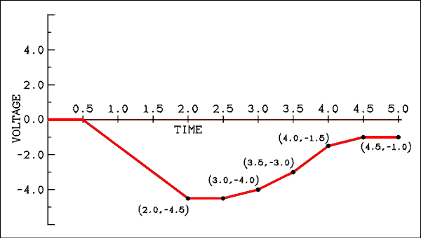
Figure 6.13 Output Voltage for Problem 14.
For a verbal description click here.
- 50 k ohms.
- 35.8 k ohm, nearest standard 5% value is 36 k ohm.
Back to Fun with Transistors.
Back to Fun with Tubes.
Back to Table of Contents.
Back to top.